-
- News
- Books
Featured Books
- pcb007 Magazine
Latest Issues
Current IssueVoices of the Industry
We take the pulse of the PCB industry by sharing insights from leading fabricators and suppliers in this month's issue. We've gathered their thoughts on the new U.S. administration, spending, the war in Ukraine, and their most pressing needs. It’s an eye-opening and enlightening look behind the curtain.
The Essential Guide to Surface Finishes
We go back to basics this month with a recount of a little history, and look forward to addressing the many challenges that high density, high frequency, adhesion, SI, and corrosion concerns for harsh environments bring to the fore. We compare and contrast surface finishes by type and application, take a hard look at the many iterations of gold plating, and address palladium as a surface finish.
It's Show Time!
In this month’s issue of PCB007 Magazine we reimagine the possibilities featuring stories all about IPC APEX EXPO 2025—covering what to look forward to, and what you don’t want to miss.
- Articles
- Columns
Search Console
- Links
- Media kit
||| MENU - pcb007 Magazine
Bowman's Micro XRF Measures Smallest Features in Wafers, Microelectronics
June 6, 2022 | BowmanEstimated reading time: 1 minute

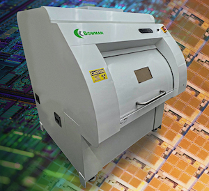
Bowman has introduced an important addition to its suite of precision XRF instruments used in the PCB, semiconductor and microelectronics industries.
The Bowman A Series Micro XRF quickly measures the smallest features on semiconductors and microelectronics. It accommodates very large PCB panels, and wafers of any size, for full sample coverage and multi-point programmable automation.
Poly-capillary optics focus the X-ray beam to 7.5 µm FWHM, the world’s smallest for XRF coating thickness analysis. A 140X magnification camera measures features on that scale; a secondary, low magnification camera provides live-viewing of samples and “birds-eye” macro-view imaging. Bowman’s proprietary dual-camera system lets operators see the entire part, click the image to zoom with the high-mag camera, and quickly identify the feature of interest.
A programmable X-Y stage with movement of 23.6 in (600 mm) in each direction can handle the largest samples in the industry. The stage has precision down to +/- 1 µm for each axis, and is used to select and measure multiple points; Bowman pattern recognition software and auto-focus features also do this automatically. The system’s 3D mapping capability can be used to view the topography of ENIG, ENEPIG, EPIG and other elite processes.
A Series instruments include 7.5 µm optics with molybdenum anode tube (chromium and tungsten also available) and a high-resolution, large-window Silicon Drift Detector (SDD) which processes more than 2 million counts per second. SDDs are the standard, industry-wide, for complex thin films. The high count rate capability is key to achieving a low minimum detection limit (MDL) and highest spectral resolution.
A Series systems are distinctive in that they are cleanroom-ready, have the largest semiconductor stage movement on the market, and are supported worldwide by a service network that provides same-day response for every benchtop XRF requirement. Equipment evaluation, selection, commissioning, maintenance and modernization is available for users of Bowman instruments, as well as other major XRF brands.
Suggested Items
Real Time with... IPC APEX EXPO 2025: MivaTek is Revolutionizing Circuit Board Manufacturing with DART Technology
04/02/2025 | Real Time with...IPC APEX EXPOBrendan Hogan from MivaTek Global discusses the company's focus on direct imaging for circuit boards and semiconductors. MivaTek is introducing DART technology for dynamic feature size adjustments. This technology enhances precision, improving registration and throughput.
Real Time with... IPC APEX EXPO 2025: Schmoll America—Committed to Supporting Customers
03/31/2025 | Real Time with...IPC APEX EXPOKurt Palmer of Schmoll America and Stephan Kunz of Schmoll Maschinen GmbH had a great show, reporting solid attendance and good opportunities, as Schmoll America celebrates its first anniversary. With a booth full of equipment for attendees to see and touch, they showcased unique products like the Pico laser and X-ray machine, and discussed plans for a new facility.
Technica USA and CBT Introducing TiTAN Hybrid at IPC APEX EXPO 2025
03/18/2025 | Technica USAThe wait is over! Technica and CBT are proud to unveil TiTAN Hybrid, a groundbreaking innovation set to redefine the PCB industry. Designed for unmatched performance, efficiency, and adaptability, this cutting-edge laser imaging technology brings the future to you—today.
Teledyne Delivers 100th Infrared Detector for the Space Development Agency's Tracking Layer
03/06/2025 | TeledyneTeledyne Technologies Incorporated, a leading provider of advanced imaging solutions, is proud to announce its continuing pattern of on-time and early deliveries for the Space Development Agency's (SDA) proliferated constellation.
Singular Photonics Emerges from Stealth with Portfolio of SPAD-based Image Sensors
01/23/2025 | PRNewswireSingular Photonics emerged from stealth mode today, launching a new generation of image sensors based on single photon avalanche diodes (SPADs). A spin-out from the University of Edinburgh lab of digital imaging pioneer