Ucamco Adds In-house Production of Large and Extra Large 'Bird of Prey' Photoplotters
June 17, 2022 | UcamcoEstimated reading time: 1 minute

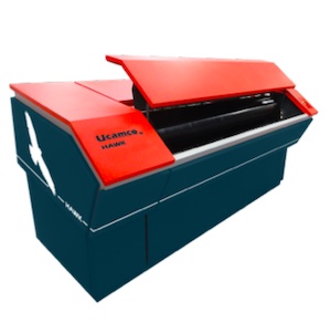
Ucamco has added the in-house production, from scratch, of new large and extra-large format laser photoplotters to its capabilities.
As the market leader in not only photoplotters, but also PCB CAM and Pre-CAM Software and Direct Imaging Systems, Ucamco is committed to keep developing PCB technology. Even more, Ucamco invests in it: "Ucamco is an expert in the field. We love to take on challenges", says Michel Van den heuvel, Product Imaging Group Director at Ucamco. "We figured we have all the human and material resources in-house to successfully build large and extra-large photoplotters. Add that to the ever-growing importance of providing full-service solutions for our customers, and the addition of this production line has really been a no-brainer.
"Our (extra) large format photoplotters are external drum laser plotters with an automatic film loader and online connection to the film processor. One of the main qualities of an excellent photoplotter is having a state-of-the-art optical-mechanical imaging unit."
"You could argue that our plotters possess the same sharp eyesight as birds of prey. Which is why we have named our brand new machines after birds with the larges wingspan - Hawk and Condor - obviously due to the size of the photoplotters."
Suggested Items
Orbel Corporation Integrates Schmoll Direct Imaging
06/04/2025 | Schmoll AmericaOrbel Corporation in Easton, PA, proudly becomes the first PCM facility in the U.S. equipped with Schmoll’s MDI Direct Imaging system. This installation empowers Orbel to support customers with greater precision and quality.
Key Insights on Photoresist for Defect Reduction
05/21/2025 | I-Connect007 Editorial TeamIn PCB manufacturing, understanding the intricacies of the photoresist process is crucial for achieving high-quality results. Industry experts Josh Krick, a technical service engineer at IEC, and Tim Blair, a PCB imaging specialist at Tim Blair LLC, share their knowledge on the essential stages of photoresist application, highlight critical advancements in materials, and discuss common defects encountered during production. They share best practices and innovative solutions to enhance the manufacturing process, reduce defects, and ensure efficiency and reliability in high-tech applications.
NXP Unveils Third-Generation Imaging Radar Processors for Level 2+ to 4 Autonomous Driving
05/09/2025 | NXP SemiconductorNXP Semiconductors N.V. unveiled its new S32R47 imaging radar processors in 16 nm FinFET technology, building on NXP’s proven expertise in the imaging radar space.
SEMICON Europa 2025 Call for Abstracts Opens for Advanced Packaging Conference and MEMS & Imaging Summit
05/05/2025 | SEMISEMI Europe announced the opening of the call for abstracts for SEMICON Europa 2025, to be held November 18-21 at Messe München in Munich, Germany. Selected speakers will share their expertise at the Advanced Packaging Conference (APC), MEMS & Imaging Sensors Summit, and during presentations on the show floor.
Summit Interconnect Hollister Elevates PCB Prototyping with New TiTAN Direct Imaging System from Technica USA
05/01/2025 | Summit Interconnect, Inc.Summit Interconnect’s Hollister facility has recently enhanced its quick-turn PCB prototyping capabilities by installing the TiTAN PSR-H Direct Imaging (DI) system.