


 The Marketing Minute: Marketing With Layers
 The Right Approach: Electro-Tek—A Williams Family Legacy, Part 1
 It’s Only Common Sense: If You’re Not Differentiated, You’re Dead


InnovationLab Demonstrates Breakthrough PCB Production Method Based on Additive Manufacturing
August 8, 2022 | InnovationLabEstimated reading time: 1 minute
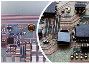
InnovationLab, the expert in printed electronics "from lab to fab", announces it has achieved a breakthrough in additive manufacturing of printed circuit boards (PCBs), helping meet higher environmental standards for electronics production while also reducing costs.
Within the research project SmartEEs2, funded by Horizon 2020, InnovationLab and its partner ISRA have developed a novel manufacturing process for copper-based solderable circuits. The circuits are screen printed and are compatible with conventional reflow processes.
Producing printed electronics is an additive process that does not use toxic etchants, and runs at comparatively low temperatures of around 150ºC, thus reducing energy consumption. Moreover, the substrates used in additive PCB manufacturing are up to 15 times thinner, compared to conventional techniques, which reduces material consumption and means the production process has less waste.
InnovationLab has so far produced a physical prototype, which includes all the important blocks of a smart label. It uses a copper ink to ensure high conductivity. Component mounting can be done in a conventional reflow soldering process, which enables manufacturers to switch to the new technology without investment in new equipment.
Multilayer layer printing, metal and dielectric, was used to produce the target functionality: a low power temperature sensor and logger, an NFC communication interface via a printed antenna, and a compact battery that is charged from a printed solar cell, making the device completely self-sufficient. The new process can produce both standard and flexible PCBs with up to four layers and can be used in product and process development for hybrid electronics.
Dr. Janusz Schinke, Head of Printed Electronics at InnovationLab, said, "This is a state-of-the-art production process, which will decrease costs and reduce logistical dependencies on suppliers, while delivering three key benefits for the environment: consuming fewer materials, using less energy, and producing less waste. By the end of this year, we expect to have scaled this process to high volumes, meeting customer demands of a million solderable tracks or more.”
SmartEEs2 is a European project, which is funded by the European Union’s Horizon 2020 research and innovation program. Its objective is to provide acceleration support to innovative companies for the integration of flexible and wearable electronics technologies, and thus to help European industry’s competitiveness.
Share on:


Testimonial
"The I-Connect007 team is outstanding—kind, responsive, and a true marketing partner. Their design team created fresh, eye-catching ads, and their editorial support polished our content to let our brand shine. Thank you all! "
Sweeney Ng - CEE PCBSuggested Items
NOVOSENSE, UAES and Innoscience Advance Power Electronics for New Energy Vehicles
10/17/2025 | PRNewswireThe partnership focuses on developing next-generation intelligent integrated Gallium Nitride (GaN) products. Leveraging their combined expertise, the new devices will deliver more reliable GaN driving and protection features, enabling higher power density and paving the way for wider adoption in automotive systems.
Jabil Announces Board Transitions
10/17/2025 | JabilJabil Inc. announced that Executive Chairman of the Board of Directors Mark T. Mondello and Directors Kathleen A. Walters and Jamie Siminoff will not seek re-election at Jabil’s Annual Meeting of Stockholders in January 2026.
StenTech Strengthens Precision Parts Platform with AME Acquisition
10/17/2025 | StenTechStenTech, North America’s leading provider of SMT printing solutions and precision manufacturing, has announced the acquisition of Advanced Metal Etching, Inc. (AME), a recognized specialist in chemically etched and laser cut precision parts.
MKS’ Atotech, ESI to Participate in TPCA Show & IMPACT Conference 2025
10/17/2025 | MKS’ AtotechMKS Inc., a global provider of enabling technologies that transform our world, announced that its strategic brands Atotech (process chemicals, equipment, software, and services) and ESI (laser systems) will showcase their latest range of leading manufacturing solutions for printed circuit board (PCB) and package substrate manufacturing at the upcoming 26th TPCA Show 2025 to be held at the Taipei Nangang Exhibition Center from 22-24 October 2025.
Rehm Wins Mexico Technology Award for CondensoXLine with Formic Acid
10/17/2025 | Rehm Thermal SystemsModern electronics manufacturing requires technologies with high reliability. By using formic acid in convection, condensation, and contact soldering, Rehm Thermal Systems’ equipment ensures reliable, void-free solder joints — even when using flux-free solder pastes.