


 The Marketing Minute: Marketing With Layers
 The Right Approach: Electro-Tek—A Williams Family Legacy, Part 1
 It’s Only Common Sense: If You’re Not Differentiated, You’re Dead


CyberOptics to Deliver Technical Presentation at the Heterogeneous Integration Summit by SEMICON Taiwan
August 16, 2022 | CyberOptics CorporationEstimated reading time: 2 minutes
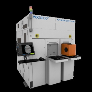
CyberOptics Corporation, a leading global developer and manufacturer of high-precision 3D sensing technology solutions will share a technical presentation at the Heterogeneous Integration Global Summit organized by SEMICON Taiwan. The company will also exhibit WaferSense and ReticleSense sensors and feature the WX3000 Metrology and Inspection system in booths I2228, I2110, I2126 and I2160 at TaiNEX 1, Taipei, September 14-16.
Dr. Subodh Kulkarni, President and CEO, CyberOptics, will present ‘High-precision 3D sensing for semiconductor bump height uniformity measurement before photo resist’ in the technical track ‘3D Heterogeneous integration (HI) driving packaging enabling technologies’ on September 16 at 2:35pm local time.
The semiconductor packaging industry continues to advance, with new designs adding more layers, finer features and more I/O channels for higher bandwidth and lower power consumption. Manufacturers face an increasing need for high-precision inspection and measurement to detect defects and improve process control.
The presentation will focus on measuring bump height uniformity before the photo resist using the NanoResolution Multiple Reflection Suppression® (MRS®) sensor technology. The unique optical architecture of the MRS sensor and the system’s proprietary image fusing and processing algorithms provide highly accurate 3D characterization that is several times faster than conventional PSP. The sensor compares data from multiple perspectives and fringe frequencies to identify and reject spurious signals from shiny and reflective surfaces, which is critical for highly accurate inspection and metrology. The presentation will also elaborate on the needs and challenges for various AP applications and how the technology can improve yields, processes and quality. ?
At the show, the company will feature the WX3000™ Metrology and Inspection system powered by the 3 µm NanoResolution MRS sensor that provides sub-micrometer accuracy on features as small as 25µm. The system is specifically designed for WLP and AP applications. While retaining its ability to reject spurious multiple reflections, it adds the ability to capture and analyze specular reflections from shiny surfaces of solder balls, bumps and pillars, allowing highly accurate inspection and metrology of these critical packaging features. Fast, 100% 3D/2D inspection and metrology can be conducted with throughput greater than 25 wafers (300mm) per hour, 2-3X faster than alternative solutions.
The new WaferSense® Auto Teaching System (ATS2) and ReticleSense® Auto Teaching System (ATRS) will also be unveiled at the show. Process and equipment engineers can speed accurate wafer and reticle hand-off teaching for proper semiconductor alignment and set-up. The thinner ATS2 and the ATSR can “see inside in real-time to capture three dimensional off-set data (x,y,z) to quickly teach wafer and reticle transfer positions – all without opening the tool. Semiconductor fabs can significantly improve their yields and processes.
Share on:


Testimonial
"Advertising in PCB007 Magazine has been a great way to showcase our bare board testers to the right audience. The I-Connect007 team makes the process smooth and professional. We’re proud to be featured in such a trusted publication."
Klaus Koziol - atgSuggested Items
Rehm Wins Mexico Technology Award for CondensoXLine with Formic Acid
10/17/2025 | Rehm Thermal SystemsModern electronics manufacturing requires technologies with high reliability. By using formic acid in convection, condensation, and contact soldering, Rehm Thermal Systems’ equipment ensures reliable, void-free solder joints — even when using flux-free solder pastes.
Indium Experts to Deliver Technical Presentations at SMTA International
10/14/2025 | Indium CorporationAs one of the leading materials providers to the power electronics assembly industry, Indium Corporation experts will share their technical insight on a wide range of innovative solder solutions at SMTA International (SMTAI), to be held October 19-23 in Rosemont, Illinois.
Knocking Down the Bone Pile: Revamp Your Components with BGA Reballing
10/14/2025 | Nash Bell -- Column: Knocking Down the Bone PileBall grid array (BGA) components evolved from pin grid array (PGA) devices, carrying over many of the same electrical benefits while introducing a more compact and efficient interconnect format. Instead of discrete leads, BGAs rely on solder balls on the underside of the package to connect to the PCB. In some advanced designs, solder balls are on both the PCB and the BGA package. In stacked configurations, such as package-on-package (PoP), these solder balls also interconnect multiple packages, enabling higher functionality in a smaller footprint.
Indium to Showcase High-Reliability Solder and Flux-Cored Wire Solutions at SMTA International
10/09/2025 | Indium CorporationAs one of the leading materials providers in the electronics industry, Indium Corporation® will feature its innovative, high-reliability solder and flux-cored wire products at SMTA International (SMTAI), to be held October 19-23 in Rosemont, Illinois.
‘Create your Connections’ – Rehm at productronica 2025 in Munich
10/08/2025 | Rehm Thermal SystemsThe electronics industry is undergoing dynamic transformation: smart production lines, sustainability, artificial intelligence, and sensor technologies dominate current discussions.