


 Beyond the Board: What Companies Need to Know Before Entering the MilAero PCB Market
 Defense Speak Interpreted: If CHIPS Cuts Back, What Happens to Electronics Packaging Funds?
 American Made Advocacy: Where’s the Budget for a Modern Military Run on Microelectronics?


CIL Expands with a New Semiconductor Packaging, Power Device and PCBA Manufacturing Facility in Andover, UK
September 5, 2022 | Custom Interconnect LtdEstimated reading time: 2 minutes
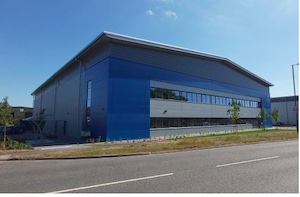
CIL is excited to announce that it is creating an advanced semiconductor packaging, power device and volume PCB Assembly (PCBA) manufacturing facility in the UK. Supported by £9M in capital investment the 46,000sq ft is in addition to its existing 34,000sq ft, giving CIL over 80,000sq ft in Andover, UK. Following the first stage six-month fit out of its ISO7 (Class 10,000) cleanroom totalling 15,000sq ft and associated offices, all of CIL’s micro-electronics production and power device development will relocate to the new facility in March 2023.
CIL has seen very strong demand for its micro-electronics and electronic assembly capability through the COVID period. Coupled with its InnovateUK supported innovation programs that are focussed on strategic areas including power device development and compound semiconductor technology, CIL has generated the demand for this investment in increased capacity and capability.
Starting with InnovateUK joint funded project “GaNSiC” in 2019 and then followed by APC15 project “@FutureBEV” in 2020, CIL has been supporting the development of GaN and SiC based power modules, discrete devices and associated power PCBA. These two projects have been catalysts to significant further R&D projects that have been supported by national funding programs including the Advanced Propulsion Centre (APC), Driving the Electric Revolution centre (DER-IC), DCMS and InnovateUK. They are all focussed on more efficient power electronics in support on Net Zero. The technologies span a range of sectors including automotive, rail, aerospace and space, 5G Communications and data-centre infrastructure. Since 2019, CIL has increased its specialist engineering department from 8 to 30 engineers with further plans to double it again over the next 3 years. This investment in engineering skills coupled with the additional unique processing equipment, will create one of the UK’s largest independent semiconductor packaging facilities, and will accommodate both world leading development labs and full volume production areas. The UK has a thriving Integrated circuit (IC) design community, but very little UK based packaging capability able to deal with development, low volume and high-volume production, the new facility is the first stage in CIL addressing this capacity requirement.
As well as the additional capacity, CIL is also increasing its process capability as it adds equipment such as a DISCO DAD 3361 dicing saw, Boschman UNISTAR Automatic Film Assisted Plastic Overmold and Scheugenpflug VDS U1000 / LP804 VDU Auto epoxy fill system with more to equipment and processes to come. Once commissioned, this equipment will enable CIL to offer UK-based wafer dicing, full device overmold service for devices such as QFN’s etc, partial device overmold and SiC and GaN based power module potting manufactured within a UK-based, UK-owned facility.
Share on:


Testimonial
"In a year when every marketing dollar mattered, I chose to keep I-Connect007 in our 2025 plan. Their commitment to high-quality, insightful content aligns with Koh Young’s values and helps readers navigate a changing industry. "
Brent Fischthal - Koh YoungSuggested Items
Nortech Systems Achieves Enhanced Fiber Optic Performance
09/16/2025 | Nortech SystemsNortech Systems Incorporated, a leading provider of design and manufacturing solutions for complex electromedical devices and electromechanical systems, announced significant advancements in its fiber optic capabilities.
Altair, Wichita State University’s NIAR Sign MoU to Accelerate Aerospace Innovation
09/16/2025 | AltairAltair, a global leader in computational intelligence, and Wichita State University’s (WSU) National Institute for Aviation Research (NIAR), one of the world’s leading aerospace research institutions, have signed a memorandum of understanding (MoU) to advance innovation across the aerospace and defense industries.
India’s Aerospace and Defence Engineered for Power, Driven by Electronics
09/16/2025 | Gaurab Majumdar, Global Electronics AssociationWith a defence budget of $82.05 billion (2025–26) and a massive $223 billion earmarked for aerospace and defence spending over the next decade, India is rapidly positioning itself as a major player in the global defence and aerospace market.
Honeywell-Led Consortium Receives UK Government Funding to Revolutionize Aerospace Manufacturing
09/02/2025 | HoneywellA consortium led by Honeywell has received UK Government funding for a project that aims to revolutionize how critical aerospace technologies are manufactured in the UK through the use of AI and additive manufacturing.
Coherent Announces Agreement to Sell Aerospace and Defense Business to Advent for $400 Million
08/15/2025 | AdventCoherent Corp., a global leader in photonics, today announced that it has entered into a definitive agreement to sell its Aerospace and Defense business to Advent, a leading global private equity investor, for $400 million. Proceeds will be used to reduce debt, which will be immediately accretive to Coherent’s EPS.