


 It’s Only Common Sense: Stay Curious, My Friends
 The Marketing Minute: AI Is Watching Your Marketing Habits


As electronic devices become smaller and smaller, the materials that power them need to become thinner and thinner. Because of this, one of the key challenges scientists face in developing next-generation energy-efficient electronics is discovering materials that can maintain special electronic properties at an ultrathin size.
Advanced materials known as ferroelectrics present a promising solution to help lower the power consumed by the ultrasmall electronic devices found in cell phones and computers. Ferroelectrics — the electrical analog to ferromagnets — are a class of materials in which some of the atoms are arranged off-center, leading to a spontaneous internal electric charge or polarization. This internal polarization can reverse its direction when scientists expose the material to an external voltage. This offers great promise for ultralow-power microelectronics.
Unfortunately, conventional ferroelectric materials lose their internal polarization below around a few nanometers in thickness. This means they are not compatible with current-day silicon technology. This issue has previously prevented the integration of ferroelectrics into microelectronics.
But now a team of researchers from the University of California at Berkeley performing experiments at the U.S.
Department of Energy’s (DOE) Argonne National Laboratory have found a solution that simultaneously solves both problems by creating the thinnest ferroelectric ever reported and the thinnest demonstration of a working memory on silicon.
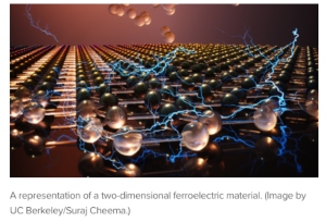
In a study published in the journal Science, the research team discovered stable ferroelectricity in an ultrathin layer of zirconium dioxide just half a nanometer thick. That’s the size of a single atomic building block, about 200,000 times thinner than a human hair. The team grew this material directly on silicon. They found ferroelectricity emerges in zirconium dioxide — normally a nonferroelectric material — when it is grown extremely thin, approximately 1-2 nanometers in thickness.
Notably, the ferroelectric behavior continues to its near-atomic-scale thickness limit of roughly half a nanometer. This fundamental breakthrough marks the world’s thinnest ferroelectric. This is surprising for a material that is not even typically ferroelectric in its bulk form.
The researchers were also able to switch the polarization in this ultrathin material back and forth with a small voltage, enabling the thinnest demonstration of a working memory ever reported on silicon. It also offers substantial promise for energy-efficient electronics, especially considering conventional zirconium dioxide is already present in today’s state-of-the-art silicon chips.
“This work takes a key step towards integrating ferroelectrics into highly scaled microelectronics,” said Suraj Cheema, a postdoctoral researcher at UC Berkeley, the first author of the study.
Visualizing the ferroelectric behavior of such ultrathin systems required the use of Argonne’s Advanced Photon Source, a DOE Office of Science user facility. ?“X-ray diffraction gives needed insight into how this ferroelectricity emerges,” said Argonne physicist John Freeland, another author of the study.
Beyond the immediate technological impact, this work also has significant implications for designing new two-dimensional materials.
“Simply squeezing 3D materials to their 2D thickness limit offers a straightforward-yet-effective route to unlocking hidden phenomena in a wide variety of simple materials,” Cheema said. ?“This greatly expands the materials design space for next-generation electronics to include materials already compatible with silicon technologies.”
As Cheema noted, simply growing just a few atomic layers of a 3D material can offer the potential for a new class of 2D materials — atomically-thin 3D materials — that go beyond conventional sheets of 2D materials like graphene. The researchers hope this work will motivate more research into two-dimensional 3D materials exhibiting emergent electronic phenomena relevant for energy-efficient electronics.
This work was led by Cheema and Sayeef Salahuddin of UC Berkeley, along with co-first authors Nirmaan Shanker and Shang-Lin Hsu. At beamline 33-BM-C of Argonne’s Advanced Photon Source, working with Argonne physicists Freeland and Zhan Zhang, the researchers employed synchrotron X-ray absorption spectroscopy and X-ray diffraction to investigate the structural evolution of ferroelectricity to the atomic scale and explore its electronic origins. At DOE’s Lawrence Berkeley National Laboratory’s Advanced Light Source and Molecular Foundry, collaborating with scientists Padraic Shafer and Jim Ciston, the material’s ferroelectric crystal structure was studied using soft X-rays and transmission electron microscopy.


