


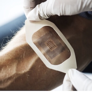


 Global PCB Connections: Rigid-flex and Flexible PCBs—The Backbone of Modern Electronics
 Flexible Thinking: The Key to a Successful Flex Circuit Design Transfer
 Happy’s Tech Talk #29: Bend-to-Install Semi-flex FR-4


Amtech Systems Books Large Repeat Order Driven by EV Growth
December 1, 2022 | Amtech Systems, Inc.Estimated reading time: 1 minute
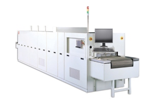
Amtech Systems, Inc., a manufacturer of capital equipment, including thermal processing and wafer polishing, and related consumables used in fabricating semiconductor devices, such as silicon carbide (SiC) and silicon power devices, analog and discrete devices, electronic assemblies and light-emitting diodes (LEDs), announced the receipt of an order for 20 controlled atmosphere furnaces for production of Direct Bond Copper (DBC) substrates.
The repeat order was received by Amtech division, BTU International, for 20 controlled atmosphere furnaces for delivery starting in the second half of fiscal 2023. These continuous furnaces will be used for the volume production of DBC substrates, a process which requires extreme control of thermal uniformity and oxidation atmosphere. The furnaces will be produced at BTU’s factory in the USA and shipped to customer locations in Asia. The DBC substrates produced by these furnaces will be used for power device modules intended for electric vehicles (EV).
“We are seeing customer demand related to the scale-up of electric vehicles across all of our divisions,” said Michael Whang, CEO of Amtech Systems. “DBC is a technology uniquely suited for heat dissipation in power modules -- and BTU’s systems have the superior process control to produce DBC substrates reliably and at scale,” added Whang.
Share on:


Testimonial
"In a year when every marketing dollar mattered, I chose to keep I-Connect007 in our 2025 plan. Their commitment to high-quality, insightful content aligns with Koh Young’s values and helps readers navigate a changing industry. "
Brent Fischthal - Koh YoungSuggested Items
Episode 6 of Ultra HDI Podcast Series Explores Copper-filled Microvias in Advanced PCB Design and Fabrication
10/15/2025 | I-Connect007I-Connect007 has released Episode 6 of its acclaimed On the Line with... American Standard Circuits: Ultra High Density Interconnect (UHDI) podcast series. In this episode, “Copper Filling of Vias,” host Nolan Johnson once again welcomes John Johnson, Director of Quality and Advanced Technology at American Standard Circuits, for a deep dive into the pros and cons of copper plating microvias—from both the fabricator’s and designer’s perspectives.
Nolan’s Notes: Tariffs, Technologies, and Optimization
10/01/2025 | Nolan Johnson -- Column: Nolan's NotesLast month, SMT007 Magazine spotlighted India, and boy, did we pick a good time to do so. Tariff and trade news involving India was breaking like a storm surge. The U.S. tariffs shifted India from one of the most favorable trade agreements to the least favorable. Electronics continue to be exempt for the time being, but lest you think that we’re free and clear because we manufacture electronics, steel and aluminum are specifically called out at the 50% tariff levels.
MacDermid Alpha & Graphic PLC Lead UK’s First Horizontal Electroless Copper Installation
09/30/2025 | MacDermid Alpha & Graphic PLCMacDermid Alpha Electronics Solutions, a leading supplier of integrated materials and chemistries to the electronics industry, is proud to support Graphic PLC, a Somacis company, with the installation of the first horizontal electroless copper metallization process in the UK.
Electrodeposited Copper Foils Market to Grow by $11.7 Billion Over 2025-2032
09/18/2025 | Globe NewswireThe global electrodeposited copper foils market is poised for dynamic growth, driven by the rising adoption in advanced electronics and renewable energy storage solutions.
MacDermid Alpha Showcases Advanced Interconnect Solutions at PCIM Asia 2025
09/18/2025 | MacDermid Alpha Electronics SolutionsMacDermid Alpha Electronic Solutions, a global leader in materials for power electronics and semiconductor assembly, will showcase its latest interconnect innovations in electronic interconnect materials at PCIM Asia 2025, held from September 24 to 26 at the Shanghai New International Expo Centre, Booth N5-E30