-
- News
- Books
Featured Books
- pcb007 Magazine
Latest Issues
Current IssueAdvancing the Advanced Materials Discussion
Moore’s Law is no more, and the advanced material solutions to grapple with this reality are surprising, stunning, and perhaps a bit daunting. Buckle up for a dive into advanced materials and a glimpse into the next chapters of electronics manufacturing.
Inventing the Future With SEL
Two years after launching its state-of-the-art PCB facility, SEL shares lessons in vision, execution, and innovation, plus insights from industry icons and technology leaders shaping the future of PCB fabrication.
Sales: From Pitch to PO
From the first cold call to finally receiving that first purchase order, the July PCB007 Magazine breaks down some critical parts of the sales stack. To up your sales game, read on!
- Articles
- Columns
- Links
- Media kit
||| MENU - pcb007 Magazine
MKS Instruments Unveils Significant Investment in its Yokohama TechCenter at Expansion Ceremony
March 14, 2023 | MKS Instruments, Inc.Estimated reading time: 2 minutes

MKS Instruments, Inc., a global provider of technologies that transform our world, unveiled a significant investment in its Yokohama Technical Center (YTC) in Japan, which will enable an industry leading integrated approach to creating solutions for complex package substrate manufacturing, satisfying current requirements as well as those needed for future roadmaps.
The YTC is an integral part of the most comprehensive portfolio of global TechCenters in the industry. These TechCenters combine unique analytical capabilities, state of the art full scale equipment, and highly proficient expert teams to conduct extensive research and development, providing world-class service to more than 8,000 customers around the globe. Working closely with customers and industry partners helps anticipate the industry’s future requirements, which in turn enables MKS to help customers stay ahead in a rapidly changing environment.
The recent investment in the YTC delivers the latest capabilities for the production of next generation package substrates. Offering a unique combination, the YTC utilizes dedicated lasers, optics, and motion systems for high precision, high-speed via formation in ABF build-up laminates, in combination with the latest process chemistry and equipment for desmear and electroless copper metallization. Using the latest Equalized Curtain Flow (ECF) plating tool, the YTC is able to support customers in their yield optimization and next generation process development for advanced packaging applications.
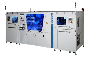
During the YTC Expansion Ceremony, Dr. John T.C. Lee, President and CEO of MKS Instruments, escorted visitors around the state-of-the-art facility showcasing the two new systems, the ESI GeodeTM A CO2 laser system and the Atotech G-Plate® plating tool, as well as demonstrating the Vitrocoat® process for Plating on Glass (PoG).
“We are highly committed to driving and leading technology development within our industries,” Dr. Lee said. “With these key installations, we are accelerating time to market through our combined capabilities, which allow us to view problems holistically and design solutions faster. This helps us to drive innovation for next generation electronic devices and offer customers and OEMs quicker development cycles for new products and materials enabling high-end SAP technology requiring <=5/5µm lines and spaces. Our unique portfolio of MKS combined services at our Yokohama technical center allows us to reduce the cycle time for a typical ABF sample from three months or more to less than one month.”
MKS Instruments’ Optimize the InterconnectSM offering drives MKS’ focus on next-generation advanced PCB and package substrate development. The investment in the YTC will further solidify MKS as a leader in the next frontier for miniaturization and complexity by enabling increasingly smaller feature sizes and offering new solutions by combining ESI laser drilling technologies with Atotech chemistry and plating equipment.
Testimonial
"We’re proud to call I-Connect007 a trusted partner. Their innovative approach and industry insight made our podcast collaboration a success by connecting us with the right audience and delivering real results."
Julia McCaffrey - NCAB GroupSuggested Items
Trouble in Your Tank: Implementing Direct Metallization in Advanced Substrate Packaging
09/15/2025 | Michael Carano -- Column: Trouble in Your TankDirect metallization systems based on conductive graphite are gaining popularity throughout the world. The environmental and productivity gains achievable with this process are outstanding. Direct metallization reduces the costs of compliance, waste treatment, and legal issues related to chemical exposure. A graphite-based direct plate system has been devised to address these needs.
Closing the Loop on PCB Etching Waste
09/09/2025 | Shawn Stone, IECAs the PCB industry continues its push toward greener, more cost-efficient operations, Sigma Engineering’s Mecer System offers a comprehensive solution to two of the industry’s most persistent pain points: etchant consumption and rinse water waste. Designed as a modular, fully automated platform, the Mecer System regenerates spent copper etchants—both alkaline and acidic—and simultaneously recycles rinse water, transforming a traditionally linear chemical process into a closed-loop system.
Driving Innovation: Depth Routing Processes—Achieving Unparalleled Precision in Complex PCBs
09/08/2025 | Kurt Palmer -- Column: Driving InnovationIn PCB manufacturing, the demand for increasingly complex and miniaturized designs continually pushes the boundaries of traditional fabrication methods, including depth routing. Success in these applications demands not only on robust machinery but also sophisticated control functions. PCB manufacturers rely on advanced machine features and process methodologies to meet their precise depth routing goals. Here, I’ll explore some crucial functions that empower manufacturers to master complex depth routing challenges.
Trouble in Your Tank: Minimizing Small-via Defects for High-reliability PCBs
08/27/2025 | Michael Carano -- Column: Trouble in Your TankTo quote the comedian Stephen Wright, “If at first you don’t succeed, then skydiving is not for you.” That can be the battle cry when you find that only small-diameter vias are exhibiting voids. Why are small holes more prone to voids than larger vias when processed through electroless copper? There are several reasons.
The Government Circuit: Navigating New Trade Headwinds and New Partnerships
08/25/2025 | Chris Mitchell -- Column: The Government CircuitAs global trade winds continue to howl, the electronics manufacturing industry finds itself at a critical juncture. After months of warnings, the U.S. Government has implemented a broad array of tariff increases, with fresh duties hitting copper-based products, semiconductors, and imports from many nations. On the positive side, tentative trade agreements with Europe, China, Japan, and other nations are providing at least some clarity and counterbalance.