-
- News
- Books
Featured Books
- smt007 Magazine
Latest Issues
Current IssueIntelligent Test and Inspection
Are you ready to explore the cutting-edge advancements shaping the electronics manufacturing industry? The May 2025 issue of SMT007 Magazine is packed with insights, innovations, and expert perspectives that you won’t want to miss.
Do You Have X-ray Vision?
Has X-ray’s time finally come in electronics manufacturing? Join us in this issue of SMT007 Magazine, where we answer this question and others to bring more efficiency to your bottom line.
IPC APEX EXPO 2025: A Preview
It’s that time again. If you’re going to Anaheim for IPC APEX EXPO 2025, we’ll see you there. In the meantime, consider this issue of SMT007 Magazine to be your golden ticket to planning the show.
- Articles
- Columns
Search Console
- Links
- Media kit
||| MENU - smt007 Magazine
Chemistry & Process Control from KYZEN at the SMTA Boise Expo
March 30, 2023 | KYZEN'Estimated reading time: Less than a minute

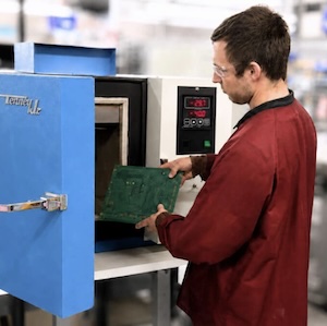
KYZEN, the global leader in innovative environmentally friendly cleaning chemistries, will exhibit at the SMTA Boise Expo & Tech Forum, scheduled to take place Tuesday, April 11, 2023 at The Grove Hotel in Boise, Idaho. Visit KYZEN for answers regarding electronics cleaning challenges. Cleaning experts will be in the booth to provide a total cleaning solution.
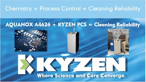
KYZEN will be highlighting their award-winning combination of chemistry and process control. For more than 30 years, KYZEN's focus has been to look at the complete process and work with them to improve that process. Their aim is to ultimately increase yields, advance reliability and help to realize cost savings along the way. KYZEN’s newest aqueous cleaning chemistry, AQUANOX A4626, paired with the KYZEN PCS accomplishes that goal.
AQUANOX A4626 is easy-to-use and control, environmentally friendly, and has a long tank life that makes it safe for multi-pass applications. Using A4626 with the KYZEN Process Control System (PCS) to monitor and automatically react to the dynamic changes in the wash bath concentration completes the process. A4626 paired with the PCS is the perfect combination – Chemistry and Control are hard at work.
Suggested Items
Scanfil Boosts Investment in Electronics Manufacturing in the US
05/08/2025 | BUSINESS WIREScanfil is investing in a second electronics manufacturing line in Atlanta, Georgia, USA. The demand for manufacturing electronics in the USA has increased over the past two years and is expected to continue growing.
ZESTRON Announces New Reliability and Solutions Service for Risk Assessment & Mitigation of Electronic Assemblies
05/06/2025 | ZESTRONZESTRON, the leading global provider of high-precision cleaning products, services, and training solutions, is thrilled to introduce its new Reliability and Solutions (R&S) service.
Trouble in Your Tank: Causes of Plating Voids, Pre-electroless Copper
05/09/2025 | Michael Carano -- Column: Trouble in Your TankIn the business of printed circuit fabrication, yield-reducing and costly defects can easily catch even the most seasoned engineers and production personnel off guard. In this month’s column, I’ll investigate copper plating voids with their genesis in the pre-plating process steps.
Knocking Down the Bone Pile: Gold Mitigation for Class 2 Electronics
05/07/2025 | Nash Bell -- Column: Knocking Down the Bone PileIn electronic assemblies, the integrity of connections between components is paramount for ensuring reliability and performance. Gold embrittlement and dissolution are two critical phenomena that can compromise this integrity. Gold embrittlement occurs when gold diffuses into solder joints or alloys, resulting in mechanical brittleness and an increased susceptibility to cracking. Conversely, gold dissolution involves the melting away of gold into solder or metal matrices, potentially altering the electrical and mechanical properties of the joint.
Happy’s Tech Talk #38: Novel Metallization for UHDI
05/07/2025 | Happy Holden -- Column: Happy’s Tech TalkI have been involved in high-density electronics substrates since 1970 when I joined Hewlett-Packard’s RF semiconductor group after college. Figure 1 shows the difference between trace/space lithography for substrates and silicon starting in 1970. My projects involved sapphire circuits for RF devices, but the figure displays the state of PCBs and integrated CMOS circuits and their packaging, not discreet RF devices. Even then, semiconductors were 50X higher density.