


 Marcy’s Musings: Operating Without a Rulebook
 It’s Only Common Sense: Hire for Hunger, Train for Skill
 Dan’s Biz Bookshelf: ‘The 'NVIDIA Way: Jensen Huang and the Making of a Tech Giant’


MKS Introduces ESI Geode A CO2 Laser System for High Precision and High-Speed ABF IC Substrate Manufacturing
May 31, 2023 | MKS Instruments, Inc.Estimated reading time: 1 minute
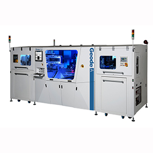
MKS Instruments, Inc., a global provider of technologies that transform our world, announced the official launch of the ESI Geode® A laser drill system today, a new configuration of the Geode® platform designed explicitly for drilling vias in the non-copper-clad ABF substrate market.
The Geode® A laser drilling system provides processing and application solutions for the FCBGA package substrate market, components which provide critical building blocks for everyday electronic devices and, in particular, high-performance computing. FCBGA substrates help enable supercomputing, artificial intelligence processing, autonomous cars, and other highly complex semiconductor modules.
“Manufacturers are under increased market pressure to deliver components that meet the precise demands of miniaturization and complexity required for advanced substrate manufacturing. At MKS, we are keenly focused on delivering the advanced technology needed for our customers to deliver next-generation productivity and quality,” said John Williams, MKS Vice President and General Manager of the ESI business. “In addition, the Geode® A laser drill is engineered as an integral component to the MKS Optimize the Interconnect SM solution, combining ESI laser drilling technologies with Atotech chemistry and plating equipment to provide customers with a full package of via formation technologies required to deliver optimal quality with the highest productivity for PCB and package substrate products.”
The Geode® A laser drilling system combines an innovative laser and optics configuration with precision pulse-shaping and beam-steering designed for ABF materials. These engineering innovations deliver the lowest cost of ownership and a greener manufacturing solution through 21% less floor space utilization, 72% less weight, and up to 65% less power consumption than the competition.
The Geode® A laser drilling system is available for purchase. More details can be found at www.esi.com, and system experts will be available at the JPCA 2023, Tokyo, Japan, May 31-June 2 in booth 6B-11.
Share on:


Testimonial
"Your magazines are a great platform for people to exchange knowledge. Thank you for the work that you do."
Simon Khesin - Schmoll MaschinenSuggested Items
Nortech Systems Launches Power over Fiber Technology Platform for EMI-Sensitive Applications
04/08/2026 | Globe NewswireNortech Systems Incorporated, a leading provider of design and manufacturing solutions for complex electromedical devices and electromechanical systems, has announced the launch of its Power over Fiber technology platform.
Flexible Thinking: Designing Flex Circuits for Dynamic Reliability
04/09/2026 | Joe Fjelstad -- Column: Flexible ThinkingFlex circuits flex. No surprises there. However, they are also very commonly designed into products because they are thin and offer consistent thickness and dielectric properties, attributes highly prized by present-day product designers of personal electronics. This would include smartphones and, increasingly, wearable electronics for medical monitoring and even fashion.
Understanding Tolerances in Flexible Circuit Design
04/01/2026 | Chris Clark, Flexible Circuit TechnologiesThe challenge with cumulative tolerances is meeting the dimensional requirements for items dimensioned on a drawing or specification for a flexible or rigid-flex circuit. It is critical to understand the fabrication processes and how features are defined when creating your tolerance requirements.
Target Condition: An Exploration of Flooding PCB Layers
04/02/2026 | Kelly Dack -- Column: Target ConditionThe concept of flooding PCB layers with copper has been around for so long, you’d think we’d have it mastered. We haven’t. (Oh, and by “we,” I mean design engineers and the software tools we depend on.) Years ago, PCB artwork was created by hand using light tables, with tape applied to Mylar. Signals were slow, traces were relatively wide, and high-current paths were simply “beefed up” with wider copper. Signal integrity wasn’t yet a driving concern. Today, solid return paths are fundamental to robust design. We understand the importance of continuous reference planes for signal integrity and EMI control.
New, Greener Solutions for Etch: Novel Copper Extraction
03/30/2026 | Richard Nichols, GreenSource Engineering“Novel” is a typical marketing phrase that implies new and unique, but often “novel” actually means an established technology being applied to a new field or application. This, in turn, is often driven by newly relevant external motivation. GreenSource has been working on just such a solution: novel copper extraction, offering a better and greener alternative to traditional LLE control systems for cupric chloride etch.