


 The Marketing Minute: Marketing With Layers
 The Right Approach: Electro-Tek—A Williams Family Legacy, Part 1
 It’s Only Common Sense: If You’re Not Differentiated, You’re Dead


Ansys Helps Accelerate Development of TMYTEK's Next-Gen mmWave Technology for 5G, Satellite Communications
July 17, 2023 | PRNewswireEstimated reading time: 1 minute
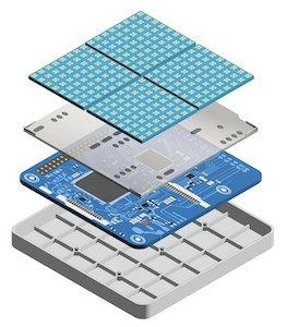
Leading mmWave technology developer TMY Technology, Inc. (TMYTEK) uses Ansys simulation software to improve the performance, efficiency, and quality of its antenna-in-package (AiP) designs through rapid design verification. TMYTEK relies on numerous Ansys solvers to improve on its next-generation mmWave technologies for 5G and satellite communications quickly — significantly reducing associated development costs.
AiP technologies integrate complex radio frequency components with their related circuitry into a single chip design — an important development in the miniaturization of the radio systems required for consumer electronics and various mmWave applications supporting 5G networks. However, application complexities and ever-increasing market demands for smaller, more compact electronics require engineers to manage and validate their AiP designs more efficiently to reduce cost and time to market.
TMYTEK relies on Ansys solutions to develop its next-generation mmWave technologies, including its 5G open radio access network (O-RAN), small cell antenna, and satellite communication user terminal electronic steering antenna designs. Ansys helps TMYTEK deliver precise results in rapid AiP performance verification, from fast, predictively accurate thermal results, to parasitic parameter calculations, to process automation.
"Using Ansys, we can offer comprehensive design services to our customers, accelerate R&D and speed time to market," said Su-Wei Chang, founder and president at TMYTEK. "Ansys solutions enable us to comprehensively simulate and measure AiP performance faster — spanning antenna and radio-frequency module parasitic parameters, thermal activity, signal and power integrity, and customized system integration design performance. This results in greater efficiency up and down the development chain, freeing time up for future projects."
"As the demand for novel mmWave solutions continues to grow, AiP design complexity and time-to-market requirements present major challenges for our customers," said John Lee, vice president and general manager of the electronics, semiconductor and optics business unit at Ansys. "Ansys simulation solutions drive the rapid innovation behind these novel mmWave technologies, such as TMYTEK's, shaping the future of 5G antenna design."
Share on:


Testimonial
"Advertising in PCB007 Magazine has been a great way to showcase our bare board testers to the right audience. The I-Connect007 team makes the process smooth and professional. We’re proud to be featured in such a trusted publication."
Klaus Koziol - atgSuggested Items
Analog Devices Launches ADI Power Studio™ and New Web-Based Tools
10/14/2025 | Analog Devices, Inc.Analog Devices, Inc., a global semiconductor leader, announced the launch of ADI Power Studio, a comprehensive family of products that offers advanced modeling, component recommendations and efficiency analysis with simulation. In addition, ADI is introducing early versions of two new web-based tools with a modernized user experience under the Power Studio umbrella:
Cadence Giving Foundation Announces Multi-Year Commitment to Expand the AI Hub at San José State University
10/13/2025 | Cadence Design Systems, Inc.The Cadence Giving Foundation today announced a multi-year commitment to expand the AI Hub at San José State University (SJSU) to equip students with the skills, hands-on training and experience needed to excel in careers in artificial intelligence (AI).
NEDME Returns October 22 — The Northwest’s Premier Design & Manufacturing Expo
10/13/2025 | NEDMEThe Northwest Electronics Design & Manufacturing Expo (NEDME) returns on Wednesday, October 22, 2025, at Wingspan Event & Conference Center, Hillsboro. The event brings together engineers, product designers, manufacturers, educators, and community partners for a full day of industry connection, learning, and networking.
Sumitomo Riko Boosts Automotive Design Efficiency 10x with Ansys AI Simulation Technology
10/13/2025 | SynopsysSumitomo Riko is implementing Ansys, part of Synopsys, Inc. AI technology to accelerate time-to-solution and improve efficiency during the design and manufacturing of automotive components.
Elementary, Mr. Watson: High Power: When Physics Becomes Real
10/15/2025 | John Watson -- Column: Elementary, Mr. WatsonHave you ever noticed how high-speed design and signal integrity classes are always packed to standing room only, but just down the hall, the session on power electronics has plenty of empty chairs? It's not just a coincidence; it's a trend I've observed over the years as both an attendee and instructor.