


 Dan’s Biz Bookshelf: ‘In Defense of a Liberal Education’
 American Made Advocacy: A Growing Presence in Washington in Turbulent Times


INSPECTIS Launches WeldInspect DIM for Welds and Shiny Surfaces
August 28, 2023 | INSPECTISEstimated reading time: 1 minute
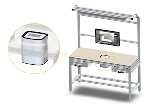
INSPECTIS AB, a global provider of advanced optical inspection solutions for industry, announces the launch of WeldInspect DIM, the world's first premium performance Digital Inverted Microscope platform specifically designed to inspect welds and other normally difficult-to-inspect shiny surfaces.
This versatile new platform opens the world of digital microscopy to many new applications. For example, precision optical and object platform alignment makes it ideal for imaging polished metal samples used in weld analysis.
In making the announcement, Alistair Gooch, Marketing and Sales Manager, said, “Weldinspect is a unique platform for advanced visual inspection tasks, utilizing Inspectis’s powerful 4K imaging. It’s ideal for viewing hybrid microcircuits, ceramic PCBs and other substrates as well. It can be used as a compact standalone instrument or coupled to a PC with powerful analytical software tools. It has everything one needs in an all-in-one Digital Inverted Microscope for weld bead analysis and measurement, including our Ultra HD imaging system with motorized zoom optics, auto-focus, built-in illumination, and dedicated software for weld measurements, documentation and reporting.”
Available with an assortment of dedicated accessories to enable a wide range of inspection tasks, and high magnification, with models providing 200x or up to 250x screen magnification, WeldInspect features built-in dedicated lighting to provide the best possible light control, premium image quality, and fast auto-focus.
The WeldInspect system includes INSPECTIS Basics software, USB3.0 or PCIe converter, 5 pcs tempered glass windows, PC communication cable and protection cover for the instrument. Dedicated weld bead measurement software bundle with Nikon NIS Elements D is ordered separately.
Share on:


Testimonial
"Our marketing partnership with I-Connect007 is already delivering. Just a day after our press release went live, we received a direct inquiry about our updated products!"
Rachael Temple - AlltematedSuggested Items
I-Connect007’s Editor’s Choice: Five Must-Reads for the Week
07/04/2025 | Marcy LaRont, I-Connect007For our industry, we have seen several bullish market announcements over the past few weeks, including one this week by IDC on the massive growth in the global server market. We’re also closely watching global trade and nearshoring. One good example of successful nearshoring is Rehm Thermal Systems, which celebrates its 10th anniversary in Mexico and the official opening of its new building in Guadalajara.
Driving Innovation: Direct Imaging vs. Conventional Exposure
07/01/2025 | Simon Khesin -- Column: Driving InnovationMy first camera used Kodak film. I even experimented with developing photos in the bathroom, though I usually dropped the film off at a Kodak center and received the prints two weeks later, only to discover that some images were out of focus or poorly framed. Today, every smartphone contains a high-quality camera capable of producing stunning images instantly.
United Electronics Corporation Advances Manufacturing Capabilities with Schmoll MDI-ST Imaging Equipment
06/24/2025 | United Electronics CorporationUnited Electronics Corporation has successfully installed the advanced Schmoll MDI-ST (XL) imaging equipment at their advanced printed circuit board facility. This significant technology investment represents a continued commitment to delivering superior products and maintaining their position as an industry leader in precision PCB manufacturing.
Orbel Corporation Integrates Schmoll Direct Imaging
06/04/2025 | Schmoll AmericaOrbel Corporation in Easton, PA, proudly becomes the first PCM facility in the U.S. equipped with Schmoll’s MDI Direct Imaging system. This installation empowers Orbel to support customers with greater precision and quality.
Key Insights on Photoresist for Defect Reduction
05/21/2025 | I-Connect007 Editorial TeamIn PCB manufacturing, understanding the intricacies of the photoresist process is crucial for achieving high-quality results. Industry experts Josh Krick, a technical service engineer at IEC, and Tim Blair, a PCB imaging specialist at Tim Blair LLC, share their knowledge on the essential stages of photoresist application, highlight critical advancements in materials, and discuss common defects encountered during production. They share best practices and innovative solutions to enhance the manufacturing process, reduce defects, and ensure efficiency and reliability in high-tech applications.