


 Trouble in Your Tank: At 40 GHz, Everything Matters, Part 1
 It’s Only Common Sense: The Underrated Business Strategy of Joy
 Punching Out: How to Stay Focused in Business and M&A


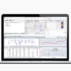
Keysight Technologies, Inc. introduces Keysight EDA 2024, a tightly integrated suite of electronic design automation (EDA) software tools that ensures first pass success. This new integrated EDA software facilitates a “shift left” approach to increase productivity for engineers developing high speed, high frequency products in multiple applications.
Shift left is an established electrical engineering practice that moves design validation forward in the development cycle to accelerate time-to-market. The rising complexity of electronic systems demands that designers complete as much validation in the virtual domain where it is easier and more cost-effective to correct functional and physical issues. Implementation of accurate modeling and simulation methodologies that create virtual prototypes and digital twins is essential to handling complexity. Key to building accurate models and faster simulations is incorporation of actual measurement data into the design and validation process in virtual space.
Keysight EDA 2024 software includes new system and circuit design workflow integration, power amplifier modeling and simulation optimization, and Satcom design evolution enhancements. The improvements expand on the software automation, intellectual property and design data management, and simulation acceleration capabilities previously announced. Powered by Keysight measurement science, the new tools provide engineers with a comprehensive solution that speeds virtual prototype creation with highly accurate validation prior to building physical prototypes and starting volume production manufacturing.
Keysight EDA 2024 software suite offers the following shift left updates:
Streamlining System and Circuit Design Workflows
The RF System Explorer integrates system architecture exploration and analysis features from SystemVue into Advanced Design System (ADS) to enable design sharing between system and circuit level workflows. RF System Explorer allocates a hierarchical subsystem and parameters to a circuit designer to change radio frequency (RF) block parameters or select the analysis path without impacting the overall architecture. Circuit designers can incorporate their circuit design or derived behavioral model into the allocated subsystem for RF verification and optimization.
Connected workflows between SystemVue and ADS enable designers to extract models of the circuit design and simulate them using RF System Explorer. Streamlined workflows provide more efficient communication between architects and subsystem engineers in enterprise teams. System architects pre-configure their own templates in SystemVue for more effective collaboration with their RF circuit design teammates. Engineering teams also avoid duplication of results visualization in ADS. The API-based tool integration maintains an open environment with the option for third-party software connectivity.
Optimizing Wide Bandgap Power Amplifier Modeling and Simulation
Like RF System Explorer’s workflow integration, the Digital Pre-Distortion (DPD) Explorer and DPD Designer tools optimize power amplifier design methodology across levels of abstraction. These tools enable power amplifier designers working on broadband applications -- including 5G FR2, DVB-S2X, and WLAN – to leverage a new Dynamic Gain Model that accounts for non-linear memory effects in topologies such as GaN Doherty.
Compact waveforms deliver unparalleled simulation speed and DPD optimization that improves the entire power amplifier design and validation process. DPD Explorer and DPD Designer utilize the same precise measurement science and algorithms found in Keysight’s PNA-X to ensure high performance results for adjacent channel power ratio (ACPR) and error vector magnitude (EVM) metrics.
Evolving Satcom Design for 5GNTN, DVB-S2X, and Phased Array Applications
SystemVue enhancements address 5G non-terrestrial network (NTN), DVB-S2X, and phased array development projects.
For 5G NTN, SystemVue updates the 5G New Radio (NR) simulation library with 1024 QAM modulation for 3GPP Release 17 and associated MCS table. The library supports full end-to-end physical layer system simulation of various NTN deployments, a new 5G channel model, and an advanced transceiver. The channel model for NTN provides all the propagation characteristics to model a variety of satellite links. It supports large path delay, large-frequency Doppler Shift, and satellite trajectory visualization.
SystemVue reduces risk, cost, and time-to-market testing satellite payload, gateway, and user equipment (UE) receiver designs with 3GPP 38.811 compliant models in simulation. Satcom system engineers can evaluate design performance under varied channel impairment conditions in minutes and optimize link closure margins. The comprehensive 5G NTN solution, including Keysight Propsim emulation and Ansys STK interoperability, enables simulation of all orbital parameters, high-velocity satellites, high-altitude platforms, and long-distance links.
For DVB-S2X, SystemVue links with Keysight Signal Studio and vector signal analysis (VSA) software tools enabling designers to create a complete digital twin for satellite digital video broadcast. The integrated solution features a new model for Satcom channel modeling, a user-friendly graphical interface that supports parameter configuration and intuitive navigation, VSA Flex Frame presets designed explicitly for DVB-S2/S2X that speed signal analysis, and DVB-S2X source and receiver supporting low signal-to-noise and bit error rate. No scripting is required to integrate the SystemVue design environment with signal generation and analysis tools in a unified simulation and testing ecosystem.
For phased array, SystemVue allows fast and easy design capture with efficient simulation of complex systems containing hundreds or thousands of RF elements and paths. SystemVue simulates active impedance correlated against Keysight and third-party finite element method (FEM) simulators. Active impedance simulation is enhanced by including X-parameters with load-pull data, which increases the modeling accuracy of the interaction between the power amplifiers and the active array impedance. Load pull modeling creates the most accurate phased array digital twin, with hardware verified by Keysight instrumentation. SystemVue has also added a new automated MDIF import capability, facilitating the consumption, manipulation, interpolation, and slicing of data such as S-parameters or other model files.
SystemVue’s powerful phased array simulation and visualization capabilities provide accurate analysis of beam directivity pattern and array configuration. Earlier insights into key beam forming metrics for optimization and decision-making saves cost by reducing expensive testing in anechoic chambers. Designers can also confirm array performance through SystemVue integration with Ansys STK for scenarios and Keysight EXata for network simulation.
Niels Faché, Vice President and General Manager, Keysight EDA, said: “Domain context matters as design engineers strive to meet rising complexity challenges and boost their productivity. The breadth of improvements we’ve packed into Keysight EDA 2024 is aimed squarely at our customers’ major pain points—faster time-to-market, first pass success, automated, integrated, and open workflows, and high speed and high frequency performance. We’ve invested heavily in software R&D to create whole product solutions spanning design, emulation, and test disciplines, and incorporating our deep workflow know-how into the early stages of product development. It’s not just plain vanilla shift left, but rather shift left powered by measurement science and application domain expertise that customers count on Keysight EDA to deliver.”


