-

- News
- Books
Featured Books
- smt007 Magazine
Latest Issues
Current Issue
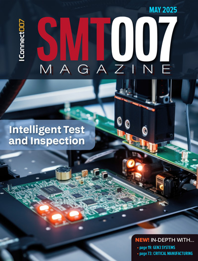
Intelligent Test and Inspection
Are you ready to explore the cutting-edge advancements shaping the electronics manufacturing industry? The May 2025 issue of SMT007 Magazine is packed with insights, innovations, and expert perspectives that you won’t want to miss.

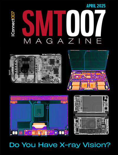
Do You Have X-ray Vision?
Has X-ray’s time finally come in electronics manufacturing? Join us in this issue of SMT007 Magazine, where we answer this question and others to bring more efficiency to your bottom line.

IPC APEX EXPO 2025: A Preview
It’s that time again. If you’re going to Anaheim for IPC APEX EXPO 2025, we’ll see you there. In the meantime, consider this issue of SMT007 Magazine to be your golden ticket to planning the show.
- Articles
- Columns
Search Console
- Links
- Media kit
||| MENU - smt007 Magazine
UHDI Fundamentals: A Primer on UHDI
September 28, 2023 | Anaya Vardya, American Standard CircuitsEstimated reading time: 4 minutes
There has always been pressure to reduce line and space as we have seen the bleeding edge technology go from 8 to 5 mils and then to 3 mils. The difference between “then” and “now” is that the prior advancements, for the most part, used the same processes, chemistry, and equipment going from 8 mils to 3 mils. But going from 3-mil to sub 1-mil trace and space is a quantum leap in printed circuit board (PCB) technology that requires a whole new set of processes and materials.
High density interconnect (HDI, the predecessor of UHDI) deals with line width and space, but primarily employs via structures to increase density. In broad terms, HDI printed circuit boards are defined as PCBs with one or more of the following via structures: microvias, stacked and/or staggered microvias, buried and blind vias, and all with sequential lamination cycles. Printed circuit board technology has been evolving with changing technology that demands smaller and faster features. HDI boards allow smaller vias, pads, lines and spaces—in other words, higher density. This increased density also allows a reduction in the number of layers and a smaller footprint. For example, one HDI board can house the functionality of multiple standard technology PCBs. Conventional state-of-the-art technology has been stuck at the 3-mil line and space capability for the longest time, but that is just not good enough to meet the increasingly tighter real estate constraints of today’s products. That is where UHDI comes in.
What is UHDI?
As soon as we cross below the 1-mil (0.001") line-width threshold, we need to stop talking in terms of mils and ounces and begin talking in terms of microns. For reference, a 3-mil trace is 75 microns, so a 1-mil trace is 25 microns. In general terms, ultra high-density interconnect (UHDI) refers to lines and spaces on a printed circuit board that are sub-25 micron. As electronics continue to shrink, so does the printed circuit board, not only in the X- and Y-axes, but also the Z-axis. Designers are challenged with reducing the form factor as well as the thickness of printed circuit boards to meet these demands.
Subtractive vs. Additive
Subtractive technology is how we have primarily produced printed circuit boards since their inception. The subtractive process refers to the selective building up of traces and features on a copper-clad substrate through plating processes, and then removing, or subtracting, the base copper to leave the circuit pattern. The limiting factor of the subtractive process is the thickness of the base copper, typically 5-micron, or 2-micron ultra-thin foil. This base copper thickness defines the minimum trace that can be achieved through the etching process. That is the technology that got us as an industry to the 3-mil line and space. The etched sidewall of the trace is tapered, not straight, with the taper getting larger the closer you get to the base substrate. The amount of taper is defined by the copper weight; the higher the weight, the more the taper. This limitation is what drove the development of UHDI technology.
UHDI additive technology starts with unclad substrate and adds an ultra-thin 0.2-micron layer of liquid ink to the substrate. The selective trace pattern is applied and the circuit pattern is then built up through the plating processes. The game changing difference here is only having to etch 2 microns of base material, which results in perfectly straight trace sidewalls.
SAP and mSAP
The semi-additive process (SAP) and modified semi-additive processes (mSAP) have been around for a while and have brought the capability of line width and space down to the 1–3 mil level. mSAP began in the IC substrate industry but has proliferated throughout PCB manufacturing shops for use with HDI products. These processes utilize a layer of base copper on the substrate between 5 and 2 microns to achieve line width reductions. However, production of sub-1-micron traces requires the ultra-thin 0.2-micron layer of liquid ink used in the A-SAP process.
A-SAP
The pioneer of UHDI processing is Averatek, which has brought its A-SAP™ process to market. A-SAP stands for “Averatek Semi-Additive Process” and is the industry leader in this technology. American Standard Circuits has partnered with Averatek on the technology which allows for the manufacture of PCBs with line width and space down to 15 microns. Some of the benefits of using A-SAP are:
- Significant size and weight reduction
- Improved reliability and signal integrity
- Improved RF performance
- Reduced costs
- Biocompatibility
These processes have allowed devices like cellphones to continually shrink in size while increasing functionality. As technology continues to push everything smaller and faster while integrating with other devices, UDHI is here for the foreseeable future.
This article originally appears in the September 2023 issue of Design007 Magazine.
Anaya Vardya is president and CEO of American Standard Circuits; co-author of The Printed Circuit Designer’s Guide to… Fundamentals of RF/Microwave PCBs and Flex and Rigid-Flex Fundamentals. He is the author of Thermal Management: A Fabricator's Perspective and The Companion Guide to Flex and Rigid-Flex Fundamentals. Visit I-007eBooks.com to download these and other free, educational titles.
Suggested Items
Kyocera Licenses Quadric’s Chimera GPNPU AI Processor IP
05/08/2025 | BUSINESS WIREQuadric announced that Kyocera Document Solutions Inc. (hereinafter: Kyocera) has licensed the Chimera™ general purpose neural processor (GPNPU) intellectual property (IP) core for use in next generation office automation system on-chip (SoC) designs.
Scanfil Boosts Investment in Electronics Manufacturing in the US
05/08/2025 | BUSINESS WIREScanfil is investing in a second electronics manufacturing line in Atlanta, Georgia, USA. The demand for manufacturing electronics in the USA has increased over the past two years and is expected to continue growing.
Cybord's Visual AI Solution to Be Integrated with Siemens' Opcenter MES
05/07/2025 | PRNewswireCybord, a leading provider of advanced visual-AI electronic component analytics, and Siemens Digital Industries Software have signed a new OEM agreement to integrate Cybord's cutting-edge AI technology with Siemens' Opcenter™ software for Manufacturing Execution Systems (MES).
SEL Announces 2025-2026 Scholarship Recipients
05/07/2025 | Schweitzer Engineering LaboratoriesSchweitzer Engineering Laboratories (SEL) is pleased to announce the latest recipients of the SEL Scholarship Program for the 2025-2026 academic year. This year, SEL has awarded 15 scholarships, each valued at $5,000, to exceptional students pursuing degrees in engineering and applied technology.
Baker Hughes' Waygate Unveils Nanotom HR for Advanced Inspection
05/06/2025 | Baker HughesWaygate Technologies, a Baker Hughes business and global leader in nondestructive testing (NDT) solutions for industrial inspection, unveiled its new extremely high-resolution computed tomography (CT) system, Phoenix Nanotom® HR (High Resolution) at the Control 2025 show in Stuttgart, Germany.


