












 The Fearless Connector: Why I Chose the Hard Road
 The Clean Truth: The Clean Truth About No-Clean Flux
 Global Sourcing Spotlight: Beyond China Plus One—Building a Truly Global Supply Network






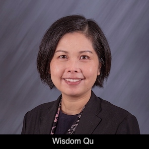
Indium Corporation Regional Product Manager Wisdom Qu will present at the iNEMI Workshop on Automotive Electronics on October 13, in Shenzhen, China.
In her presentation Low-Voiding, High-Reliability, Lead-Free Solder Paste Design for Automotive Applications, Qu will examine the results of a test comparing a solder paste based on a mixed powder technology, containing Sn/Ag/Cu/Bi/Sb/In in the final joint, with SAC305 and other high-reliability pastes. The voiding from a QFN package was consistently lower than 15%, which is better than SAC305. TCT reliability under AEC Grade 1 for BGA192, QFN, and chip-resistor also demonstrated improved reliability compared to SAC305 and the other high-reliability alloys.
With the rapid growth of the 5G and EV markets, the electronics industry has higher requirements for product reliability, with the extended lifetime under AEC Grade 1 or even Grade 0 conditions. Traditional high-reliability solder alloys contain five or six elements or even more, which strengthens through solid solution and/or precipitate solution.
“The microstructural complexity of the multi-element high-reliability alloys makes the melting behavior complicated, which may lead to worsened voiding performance compared to traditional SAC305 after reflow,” said Qu. “Designing the solder paste with mixed powder technology can reduce voiding by using at least one ternary or quaternary alloy powder constituent in the paste while the final joint is still a quinary or even senary alloy system.”
As Regional Product Manager for PCB Assembly Solder Paste in Asia, Qu facilitates business development and growth of PCB assembly product offerings, focusing on solder paste. A certified SMT process engineer, she has more than 17 years of experience in surface mount technology and earned a degree in mathematics from Hubei Radio and Television University in China.


