


 American Made Advocacy: Five Years of Educating, Advocating, and Influencing Legislation and Policy
 Defense Speak Interpreted: Understanding What the Department of Defense Is, and Isn’t
 The Right Approach: The End of an Era—DoD Proposes MIL-PRF-31032 Cancellation


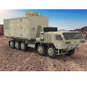
Lockheed Martin was awarded a contract to develop and deliver up to four 300 kW-class laser weapon systems to the U.S. Army’s Indirect Fire Protection Capability-High Energy Laser (IFPC-HEL) prototype program. The IFPC-HEL system complements other layered defense components to protect soldiers from stressing threats, unmanned aerial systems, rocket, artillery and mortars, along with rotary and fixed-wing aircraft.
“Winning the IFPC-HEL prototype contract is the result of several years of complex program evolution, strategic investments and partnership with the Army on this program,” said Rick Cordaro, vice president of Lockheed Martin Mission Systems & Weapons. “Our mature directed energy technology enables Lockheed Martin to provide speed, agility, and 21st Century Security solutions to the Army.”
Lockheed Martin will deliver two 300 kW-class IFPC-HEL prototypes with an option for two additional 300 kW-class units.
The Evolution of IFPC-HEL
- Since 2019, Lockheed Martin was integral to the transition from the 100 kW-class science and technology program, the High Energy Laser Tactical Vehicle Demonstrator (HEL-TVD), to deliver a 300 kW-class IFPC-HEL demonstrator.
- In 2020, Lockheed Martin was awarded a contract to develop a compact, ruggedized 300 kW-class laser for the Department of Defense.
- In August of 2022, Lockheed Martin delivered the High Energy Laser Scaling Initiative (HELSI) laser for use in the IFPC-HEL demonstrator, which was the most powerful solid-state directed energy technology delivered at that time.
Our Directed Energy Legacy
Our 300 kW-class laser weapon system design and build was enabled by significant investments in directed energy technology and the contributions of a dedicated team. Lockheed Martin applies more than 40 years of experience in the research, design, development, and capture of electromagnetic energy to elevate its power for innovative 21st Century Security solutions.


