


 Global Citizenship: The Global Push for Digital Inclusion
 Knocking Down the Bone Pile: Addressing End-of-life Component Solderability Issues, Part 4
 The Knowledge Base: A Conference for Cleaning and Coating of Mission-critical Electronics


AT&S Welcomes the Austrian Government’s Clear Commitment to Microelectronics
October 31, 2023 | AT&SEstimated reading time: 2 minutes
The Styria-based microelectronics manufacturer AT&S welcomes the announcement of the Austrian Federal Government to endow investments in the country’s microelectronics industry with three billion euros up until 2031. These funds are an important step towards Europe’s technological independence and lay the foundation for sustainable growth in economic sectors that will be crucial in the future. The current draft budget provides for funding the Austrian microelectronics industry with a total of three billion euros in the next seven years. The new budget, which will be definitively adopted in November, also includes additional funds from the Federal Ministry of Labour and Economy amounting to 50 million euros, which will increase the funds available in Austria for the European funding project IPCEI ME/CT (II) (Important Projects of Common European Interest) to 255 million euros.
“Austria is a leading location for microchips in Europe. As a result, the number of future-oriented jobs will expand in the long term, generating prosperity. With nearly three billion euros to be invested in the coming years, we can support research and new investments of semiconductor companies along the entire value chain in Austria,” Economics Minister Martin Kocher said last week.
AT&S has long been engaged in efforts to create internationally competitive framework conditions for the microelectronics industry in Austria. “We are pleased with the government’s clear commitment to an industrial policy focus on microelectronics. Without microelectronics, there will be no digitalization, no green energy transition and no sustainable growth. If Europe and Austria want to prevail in global competition, we must create the right conditions. Such bold investments in Austria, combined with the European funding programmes, provide a good foundation. Now we have to keep working to build know-how and capacities along the entire value chain,” says AT&S CEO Andreas Gerstenmayer.
Styrian heart for Europe’s microelectronics
The additional funds complement the investments made by AT&S as part of the European IPCEI programs and in the future also as part of the Chips Act. The first IPCEI for microelectronics, which AT&S recently completed, resulted, among other things, in the development of power-saving energy supply for electric cars and a new copper recycling plant, which is already successfully used at the AT&S plant in Leoben.
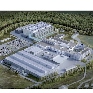
The second IPCEI for microelectronics ME/CT (II) is currently running and now provides Austrian companies with a total of 225 million euros for research, development and building industrial capacities. As part of IPCEI ME/CT (II), AT&S is investing more than half a billion euros in building a research and production centre for IC substrates and packaging technologies in Leoben, which is unique in Europe.
Share on:


Suggested Items
Chiplets and the Like are Redefining Microelectronics
06/25/2025 | productronicaThe performance of modern AI and high-performance computing applications can only be achieved with high-performance semiconductor technology.
STMicroelectronics Introduces Advanced Human Presence Detection Solution to Enhance Laptop and PC User Experience
06/24/2025 | STMicroelectronicsSTMicroelectronics, a global semiconductor leader serving customers across the spectrum of electronics applications, introduces a new Human Presence Detection (HPD) technology for laptops, PCs, monitors and accessories, delivering more than 20% power consumption reduction per day in addition to improved security and privacy.
ULVAC Continues Participation in 'Lab-in-Fab' Project to Advance Piezoelectric MEMS Technology, Now Entering a New Phase
06/19/2025 | JCN NewswireULVAC, Inc. announced that the collaborative development project "Lab-in-Fab," aimed at advancing piezoelectric Micro-Electro-Mechanical Systems (piezoMEMS) technology and in which ULVAC has participated since 2020, is entering a new phase. ULVAC will continue its participation in this initiative, contributing to the commercialization of piezoMEMS by providing deposition and etching technologies as an equipment manufacturer.
American Made Advocacy: Supporting the Entire PCB Ecosystem—Materials to OEMs
06/17/2025 | Shane Whiteside -- Column: American Made AdvocacyWith the addition of RTX to PCBAA’s membership roster, we now represent the interests of companies in the entire PCB ecosystem. From material providers to OEMs, the insights of our collective members help us educate, advocate, and support legislation and policy favorable to America’s microelectronics manufacturers. The industry veterans who lead these companies provide valuable perspective, and their accumulated wisdom makes us an even stronger association.
Enough Talk—Time to Strengthen America’s Microelectronics Industrial Base
06/09/2025 | James Will, USPAEThe U.S. doesn’t have an innovation problem in terms of microelectronics, or a talent problem or even an investment problem. What the U.S. has is a coordination problem, and that’s threatening the livelihood of our domestic microelectronics ecosystem.