


 American Made Advocacy: PCBs in the National Spotlight
 Defense Speak Interpreted: Extreme Financial Disparity in Drones and Missiles
 The Right Approach: The End of an Era—DoD Proposes MIL-PRF-31032 Cancellation


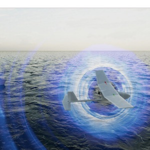
The Office of Naval Research (ONR) has awarded BAE Systems' FAST LabsTM research and development organization a $5 million contract for the COALESCE (Common-architecture Amplifier for Low-cost, Efficient, SWaP-Constrained Environments) program.
In this effort, BAE Systems' FAST Labs, will develop advanced Gallium Nitride (GaN)-based monolithic microwave integrated circuit (MMIC) and module electronics. The program's objective is to develop the world's highest efficiency high power amplifier module in its frequency band. The radio-frequency (RF) modules will then transition to small form factor U.S. Navy payloads, enabling longer range and greater effectiveness in active electronic warfare applications.
"The COALESCE program closes the gap between commercial electronics and customized electronics to meet the Department of Defense's space and power requirements and enable next-generation solutions," said Ben McMahon, technology development manager at BAE Systems' FAST Labs. "Together with the Office of Naval Research, we will deliver these electronic solutions to increase survivability for our warfighters."
BAE Systems will provide capabilities above and beyond what can be found commercially, and its solution is designed specifically for harsh DoD operating environments. The technology's high power and ultra-small form factor will enable next-generation radar, electronic warfare, and communication applications.
MMICs and modules for the program will be fabricated at BAE Systems' Microelectronics Center Foundry in Nashua, New Hampshire. The FAST Labs organization in Merrimack, New Hampshire will work to ensure the technology is relevant across multiple DoD branches, applications, and businesses.


