


 It’s Only Common Sense: Creativity Is Noisy, Messy, and So Worth It
 Dan’s Biz Bookshelf: ‘The Soul of a New Machine’


The global high-tech company AT&S develops and produces pioneering connection technologies. However, AT&S products and the highly complex technology behind them are usually invisibly installed in the end devices of AT&S customers.
In order to make the invisible visible and the intangible tangible, AT&S has installed a spectacular Erlebniswelt (“world of experience”) in Hinterberg and officially opened it on December 13. As an international partner school of AT&S, the Europagymnasium Leoben was given an exclusive first glimpse into this world to test the educational concept first-hand.
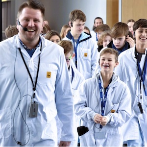
The youngsters’ journey began in the foyer of the NWW with an interactive world map showing all AT&S locations, video installations, a career building block generator, a selfie station, an oversized circuit board layer model and a dizzying simulation flight in the 3D cinema through the inside of a smartphone – right up to the selfie flash. Afterwards, the school class were given white work coats and set off with an AT&S guide to the multimedia stations in production, past cleanroom employees and the physics laboratory and with a brief look at HTB3, the new competence center for IC substrates in Europe, which will open in 2024.
First class feedback
AT&S tour guide Christopher Kaiser, Training Coordinator, had plenty of exciting facts to spread, and the students were very attentive, as the feedback round proved. Moritz (13) had even memorized technical details: “I was most impressed by the 3D cinema, the glowing conductor paths at the entrance, the cleanroom suits and the fact that you can press almost 100 layers into one printed circuit board.” His classmate David (13) was amazed: “I didn’t expect to learn so much today. Everyone was very nice. We even got a little present at the end.” Christian (13) summarized: “The Erlebniswelt is very child-friendly and you get a great glimpse into the company. The technological modern age was explained to us in a great way and we were even able to watch the employees at work, which was very fascinating, all in all a wonderful visit.” Alina (13) from Niklasdorf spoke was also enthusiastic about AT&S technology: “The employees in the cleanroom suit and the 3D cinema were really great. My uncle worked at AT&S for years and now I know what the company looks like from the inside.”
Complex topic, experienced at first hand
For Carina Pusch, class teacher of the 3rd grade at Europagymnasium Leoben, the educational concept of the Erlebniswelt is a great addition to the lessons at school: “The AT&S Erlebniswelt is very impressive because the complex topic of microelectronics can be experienced and touched up close. AT&S manages to explain high-tech to young students. You don’t need an advanced degree in science to understand what it’s all about. My students were totally enthusiastic.”
The AT&S Erlebniswelt was conceived in collaboration with SFG, the Styrian Business Promotion Agency, as a project of Erlebniswelt Wirtschaft, an initiative of the Province of Styria, and implemented with Creative Industries Styria (CIS) and the design agencies “look! design” and “Ars Electronica Futurelab”. From January 2024, the Line Tours will be available to all visitors, not just school classes, upon registration.
Tour facts
- Language: German/English
- Duration: 90 min.
- Groups: max. 15 people, school classes please enquire separately
- Age: recommended from 10 years
- Free admission
- Limited accessibility


