


 Beyond the Board: Early Engagement Means Faster Prototyping for Defense Programs
 Defense Speak Interpreted: The Autonomous Plane Battle—Skyborg Vs. Loyal Wingman
 American Made Advocacy: Congress Back from Break With Work To Do


Intel Opens Fab 9 in New Mexico
January 25, 2024 | IntelEstimated reading time: 2 minutes
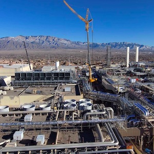
Intel celebrated the opening of Fab 9, its cutting-edge factory in Rio Rancho, New Mexico. The milestone is part of Intel's previously announced $3.5 billion investment to equip its New Mexico operations for the manufacturing of advanced semiconductor packaging technologies, including Intel’s breakthrough 3D packaging technology, Foveros, which offers flexible options for combining multiple chips that are optimized for power, performance and cost.
“Today, we celebrate the opening of Intel’s first high-volume semiconductor operations and the only U.S. factory producing the world’s most advanced packaging solutions at scale. This cutting-edge technology sets Intel apart and gives our customers real advantages in performance, form factor and flexibility in design applications, all within a resilient supply chain. Congratulations to the New Mexico team, the entire Intel family, our suppliers, and contractor partners who collaborate and relentlessly push the boundaries of packaging innovation,” said Keyvan Esfarjani, Intel executive vice president and chief global operations officer.
Intel’s global factory network is a competitive advantage that enables product optimization, improved economies of scale and supply chain resilience. The Fab 9 and Fab 11x facilities in Rio Rancho represent the first operational site for mass production of Intel’s 3D advanced packaging technology. It is also Intel's first co-located high-volume advanced packaging site, marking an end-to-end manufacturing process that creates a more efficient supply chain from demand to final product.
Fab 9 will help fuel the next era of Intel’s innovation in advanced packaging technologies. As the semiconductor industry moves into the heterogeneous era that uses multiple “chiplets” in a package, advanced packaging technologies, such as Foveros and EMIB (embedded multi-die interconnect bridge), offer a faster and more cost-efficient path toward achieving 1 trillion transistors on a chip and extending Moore’s Law beyond 2030.
Foveros, Intel’s 3D advanced packaging technology, is a first-of-its-kind solution that enables the building of processors with compute tiles stacked vertically, rather than side-by-side. It also allows Intel and foundry customers to mix and match compute tiles to optimize cost and power efficiency.
"This investment by Intel underscores New Mexico’s continued dedication to bring manufacturing back home to America," said Gov. Michelle Lujan Grisham. "Intel continues to play a key role in the state’s technology landscape and strengthen our workforce, supporting thousands of New Mexico families.”
The $3.5 billion investment in Rio Rancho has created hundreds of high-tech Intel jobs, more than 3,000 construction jobs and an additional 3,500 jobs across the state.
Share on:


Testimonial
"Your magazines are a great platform for people to exchange knowledge. Thank you for the work that you do."
Simon Khesin - Schmoll MaschinenSuggested Items
MKS’ Atotech, ESI to Participate in TPCA Show & IMPACT Conference 2025
10/17/2025 | MKS’ AtotechMKS Inc., a global provider of enabling technologies that transform our world, announced that its strategic brands Atotech (process chemicals, equipment, software, and services) and ESI (laser systems) will showcase their latest range of leading manufacturing solutions for printed circuit board (PCB) and package substrate manufacturing at the upcoming 26th TPCA Show 2025 to be held at the Taipei Nangang Exhibition Center from 22-24 October 2025.
Advanced Semiconductor Packaging Market Sees Rising Adoption Across Automotive and Industrial Sectors
10/14/2025 | openPRThe semiconductor packaging market size is estimated to reach at a CAGR of 7.2% during the forecast period (2024-2031).
Interposers, Substrates, and Advanced Manufacturing
10/13/2025 | Marcy LaRont, I-Connect007I attend a lot of industry trade shows and conferences. Lately, during conversations with technologists, I’ve noticed that there is some confusion about what exactly constitutes an interposer. One question I hear every so often is, “Are all interposers substrates?” The short answer to that question is no. But some interposers are, in fact, full substrates.
I-Connect007 Editor’s Choice: Five Must-Reads for the Week
10/10/2025 | Nolan Johnson, I-Connect007I-Connect007 has a new monthly digest newsletter, the Advanced Electronic Packaging Digest, and as I was scanning our advanced packaging newsfeeds this week, I came across a primer from tokenring.ai (republished through station WRAL, Raleigh, North Carolina), which I found quite useful. Whether you’re a designer, fabricator, or assembler, the package schemes being developed will change how you work, so be sure to keep your eye on the technological horizon and subscribe to the monthly Advanced Electronic Packaging Digest.
The Latest Issue: Advanced Electronics Packaging Digest to Explore Critical Minerals, Substrates, and Reliability Standards Driving Next-Gen Electronics
10/09/2025 | I-Connect007I-Connect007 is pleased to announce the upcoming issue of Advanced Electronics Packaging Digest (AEPD) on October 13, 2025, featuring expert insights on the technologies shaping the future of advanced packaging. As the electronics industry evolves, this issue takes a closer look at the materials, designs, and standards redefining performance and reliability across global markets.