


 It’s Only Common Sense: Marketing Isn’t Fluff, It’s Ammunition
 Driving Innovation: Mechanical and Optical Processes During Rigid-flex Production
 The Chemical Connection: Onshoring PCB Production—Daunting but Certainly Possible


Dynamic Grid Orders Hentec Industries/RPS Automation Valence 3508 Selective Soldering System
February 22, 2024 | Hentec Industries/RPS AutomationEstimated reading time: Less than a minute
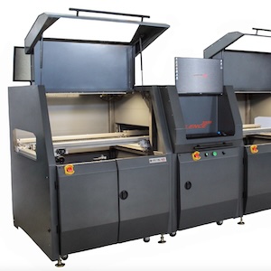
Hentec Industries/RPS Automation, a leading manufacturer of selective soldering, lead tinning and solderability test equipment, is pleased to announce that Dynamic Grid has ordered a Hentec Industries/RPS Valence 3508 selective soldering system.
The Valence 3508 is designed for high-mix, high-volume, advanced level PCB production. The continuous duty, multi-station, in-line selective soldering system utilizes an electromagnetic solder pump. The Hentec/RPS Valence 3508 can be programmed in minutes and is highly configurable and customizable. With a three-station processing area and stainless-steel ball screws, the Valence 3508 selective soldering system increases production efficiency and reduces downtime associated with periodic preventive maintenance.
Share on:


Testimonial
"We’re proud to call I-Connect007 a trusted partner. Their innovative approach and industry insight made our podcast collaboration a success by connecting us with the right audience and delivering real results."
Julia McCaffrey - NCAB GroupSuggested Items
Aircraft Wire and Cable Market to surpass USD 3.2 Billion by 2034
10/30/2025 | Global Market Insights Inc.The global aircraft wire and cable market was valued at USD 1.8 billion in 2024 and is estimated to grow at a CAGR of 5.9% to reach USD 3.2 billion by 2034, according to recent report by Global Market Insights Inc.
The Training Connection Continues to Grow with Addition of Veteran IPC Trainer Bill Graver
10/30/2025 | The Training Connection LLCThe Training Connection, LLC (TTC-LLC), a premier provider of test engineering and development training, is proud to announce the addition of Bill Graver to its growing team of industry experts. A respected professional with more than 35 years in electronics manufacturing, Bill joins as an IPC Master Trainer, bringing a wealth of hands-on experience in PCB testing, failure analysis, and process improvement.
I-Connect007 Welcomes New Columnist: Leo Lambert, EPTAC
10/30/2025 | I-Connect007I-Connect007 is excited to announce a column by Leo Lambert, an industry veteran with 40 years of experience, an award winner, and technical director at EPTAC. This column, Learning With Leo, will explore the evolution and related challenges of electronics product assembly, especially as it relates to training.
On the Line With… Ultra HDI Podcast—Episode 7: “Solder Mask: Beyond the Traces,” Now Available
10/31/2025 | I-Connect007I-Connect007 is excited to announce the release of the seventh episode of its 12-part podcast series, On the Line With… American Standard Circuits: Ultra HDI. In this episode, “Solder Mask: Beyond the Traces,” host Nolan Johnson sits down with John Johnson, Director of Quality and Advanced Technology at American Standard Circuits, to explore the essential role that solder mask plays in the Ultra HDI (UHDI) manufacturing process.
AI Triggers Next Paradigm Shift in PDN
10/23/2025 | Istvan Novak, SamtecArtificial intelligence (AI), together with machine learning (ML), is creating an unprecedented surge of computing and networking infrastructure needs. This, in turn, has dramatically increased the power consumption of computing and networking chips.