















 Marcy’s Musings: A Frighteningly Good October Issue
 It’s Only Common Sense: Win the Sale Before the RFQ Arrives
 The Marketing Minute: Marketing Is a Team Sport





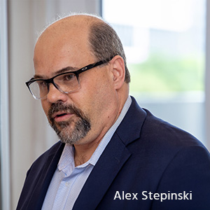
In this interview, Alex Stepinski delves into the evolving landscape of additive manufacturing technology in PCB fabrication. He highlights the historical shifts in additive and subtractive processes and emphasizes the recent focus on fine patterning and 3D printing. He discusses the challenges faced in achieving fully additive processes, citing past experiences and the need for extensive process control. The conversation also explores the drivers and barriers to adoption, with Alex underscoring the importance of OEM involvement and targeted marketing efforts.
Marcy LaRont: Alex, as high-density PCB requirements move to sub-25 micron features, traditional subtractive PCB processes simply cannot get us there. Let’s talk about additive manufacturing technology as it relates to PCB manufacturing: What are its advantages, disadvantages, and costs, and where that technology seems to be headed?
Alex Stepinski: Additive processes have been part of PCB fabrication since the beginning. Industry has basically just vacillated the ratio of subtractive to additive over time.
It changes based on production and process strategies. As always, there is the consideration of how to get where you need to be technologically, with reliability, and with the equipment you already have. Historically, companies have approached their manufacturing differently. Some companies were all panel plating. Some companies were all pattern plating, and some were a mix of the two. Today, you have a synthesis of both.
Recent discussions around additive have focused on very fine patterning, which forces a higher ratio of additive plating than historically has been commonly experienced in the market. The other aspect is 3D printing, an additive method that's been growing in recent years. We started talking about solder mask 20 years ago. Finally, some companies are leading the way in advanced 3D printing of solder mask.
Now, we are also starting to see additive in materials in conductive and dielectric layers. There are a host of different additive processing methods being applied today. There is still a lot of due diligence that needs to be done. In 2013, I helped build the first additive factory globally. It was 100% inkjet for resists and solder mask. No one has done a fully additive facility since that time. It worked very well for low-tech products. The challenge was that the process window was very small and required a lot of customization. Unfortunately, that inkjet supplier went out of business years later because nobody else could hold the process window that tightly without an inline process like ours.
To really have a fully additive process, and not just 3D printing, you need a lot of process control that we don't generally have in the market.
Barry Matties: It seems like you are describing a process engineer, someone who pays close attention to monitoring and controlling processes. Do you see a lack of process engineers?
Alex Stepinski: What I am talking about with the additive factory example is a case study from 10 years ago. A lot of process development was needed to identify the process control specifications. Once that was done, we were able to hold the specifications without significant supervision. Unfortunately, a lot of what we learned back then relative to additive is lost knowledge. From what I've seen in the market, people are relearning many of those lessons now. Adoption is still in its infancy, but I am happy to see it finally picking up.
To read this entire conversation, which appeared in the May 2024 issue of PCB007 Magazine, click here.


