-

-
News
News Highlights
- Books
Featured Books
- smt007 Magazine
Latest Issues
Current Issue
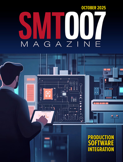
Production Software Integration
EMS companies need advanced software systems to thrive and compete. But these systems require significant effort to integrate and deploy. What is the reality, and how can we make it easier for everyone?

Spotlight on India
We invite you on a virtual tour of India’s thriving ecosystem, guided by the Global Electronics Association’s India office staff, who share their insights into the region’s growth and opportunities.

Supply Chain Strategies
A successful brand is built on strong customer relationships—anchored by a well-orchestrated supply chain at its core. This month, we look at how managing your supply chain directly influences customer perception.
- Articles
- Columns
- Links
- Media kit
||| MENU - smt007 Magazine
Samsung Electronics to Provide Turnkey Semiconductor Solutions with 2nm GAA process and 2.5D Package to Preferred Networks
July 9, 2024 | BUSINESS WIREEstimated reading time: 2 minutes
Samsung Electronics Co., Ltd., a world leader in advanced semiconductor technology, announced that it will provide turnkey semiconductor solutions using the 2-nanometer (nm) foundry process and the advanced 2.5D packaging technology Interposer-Cube S (I-Cube S) to Preferred Networks, a leading Japanese AI company.
By leveraging Samsung’s leading-edge foundry and advanced packaging products, Preferred Networks aims to develop powerful AI accelerators that meet the ever-growing demand for computing power driven by generative AI.
Since starting mass production of the industry’s first 3nm process node applying Gate-All-Around (GAA) transistor architecture, Samsung has strengthened its GAA technology leadership by successfully winning orders for the 2nm process with further upgrades in performance and power efficiency.
The cooperation with Preferred Networks marks the first achievement for Japanese companies in the field of large-sized heterogeneous integrated package technologies and Samsung plans to accelerate its leading global advanced package market offensive.
The 2.5D Advanced Package I-Cube S technology included in the turnkey solutions, is a heterogeneous integration package technology, with multiple chips in one package to enhance inter-connection speed and reduce package size. The use of the silicon interposer (Si-interposer) is crucial in achieving ultra-fine redistribution layer (RDL) and stabilizing power integrity for optimal semiconductor performance. GAONCHIPS, a specialized system semiconductor development company, designed the chip.
"We are excited to lead in AI accelerator technology with Samsung Electronics’ 2nm GAA process. This solution will significantly support Preferred Networks’ ongoing efforts to build highly energy-efficient, high-performance computing hardware that meets the ever-growing computing demands from generative AI technologies, especially large language models.,” said Junichiro Makino, VP and Chief Technology Officer (CTO) of Computing Architecture at Preferred Networks.
"This order is pivotal as it validates Samsung's 2nm GAA process technology and Advanced Package technology as an ideal solution for next-generation AI accelerators," said Taejoong Song, Corporate VP and the head of Foundry Business Development Team at Samsung Electronics. "We are committed to closely collaborating with our customers ensuring that the high performance and low power characteristics of our products are fully realized."
Preferred Networks, headquartered in Tokyo, develops advanced software and hardware technologies by vertically integrating the AI value chain from chips to supercomputers and generative AI foundation models. It provides solutions and products for various industries such as manufacturing, transportation, healthcare, entertainment, and education. The company is one of the major players in the global AI market, achieving first place three times in the past five years on the Green500 list of supercomputers.
Based on this collaboration, Samsung and Preferred Networks plan to showcase groundbreaking AI chiplet solutions for the next-generation data center and generative AI computing market in the future.
Testimonial
"We’re proud to call I-Connect007 a trusted partner. Their innovative approach and industry insight made our podcast collaboration a success by connecting us with the right audience and delivering real results."
Julia McCaffrey - NCAB GroupSuggested Items
KYZEN Brings Reliability to Life at productronica 2025 with ANALYST² Process Control Demos
10/22/2025 | KYZEN'KYZEN, the global leader in innovative environmentally responsible cleaning chemistries, will exhibit at productronica 2025, November 18–21 in Munich, Germany, where the company will put a spotlight on its award-winning KYZEN ANALYST² process control system in Hall A4, Stand 450.
SCHMID Group Secures Major Orders for AI Server PCB Production Equipment
10/22/2025 | SCHMID GroupSCHMID Group, a global equipment maker and solution provider for Printed Circuit Boards (PCB) and IC-Substrate manufacturing – announced the successful acquisition of two significant orders in the fast-growing field of PCB for artificial intelligence (AI) server applications. So called AI-Server-Boards.
SEMICON Japan 2025 to Spotlight Sustainability in AI and Semiconductor Innovation
10/22/2025 | SEMISEMICON Japan 2025, the largest gathering of leaders from the microelectronics manufacturing supply chain in Japan, will bring together more than 1,200 exhibitors showcasing semiconductor solutions from December 17-19 at Tokyo Big Sight.
Circus SE Set for High-Volume Market Entry in the Defense Sector
10/17/2025 | BUSINESS WIRECircus SE a global technology leader in AI robotics for autonomous nutrition systems and troop supply, is expanding its global production network as part of its high-volume market entry into the defense sector.
China Expands Rare Earth Export Restrictions, Tightening Grip on Global Supply Chains
10/16/2025 | I-Connect007 Editorial TeamChina sharply expanded its rare earth export restrictions on Oct. 9, adding additional elements and refining technologies to its control list while imposing stricter rules on foreign users in the defense and semiconductor industries.


