


 Standard of Excellence: The Future of Fabrication—From Art to Automation
 Knocking Down the Bone Pile: The Business Case for Component Reclamation
 Global Sourcing Spotlight: The Hidden Power of the Rep Network


Nordson Electronics Solutions, a global leader in electronics manufacturing technologies, will feature the latest technologies in fluid dispensing for semiconductor advanced packaging at the SEMICON Taiwan tradeshow, booth L0516.
On display will be the ASYMTEK Forte® fluid dispensing system, configured for high productivity and accuracy for many semiconductor packaging and microelectronics manufacturing applications. The Forte system is ideal to tackle high-volume underfill, dispense gap fill, and sealing lines for fan-out/fan-in, strips, and module assembly.
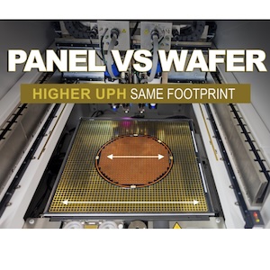
Other featured technologies include developments for high-throughput panel-level packaging (PLP) and wafer-level packaging (WLP), and handling the challenges of warpage during fluid dispensing operations. Presentations will be available to show different configurations for WLP and PLP on the ASYMTEK Vantage® fluid dispensing system, and how these systems can successfully ensure precise dispense results with high throughput.
Experts will be ready to discuss how Nordson can support your manufacturing of reliable semiconductor products. SEMICON Taiwan will be held at TaiNEX, Taipei Taiwan, September 4-6, 2024.
Especially for wafer-level and panel-level packaging, these technologies ensure high-throughput, precise dispense results within the same footprint as current equipment.


