


 The Marketing Minute: Marketing With Layers
 The Right Approach: Electro-Tek—A Williams Family Legacy, Part 1
 It’s Only Common Sense: If You’re Not Differentiated, You’re Dead


Global Semiconductor Packaging Material Market Outlook Shows Return to Growth Starting in 2024
October 2, 2024 | SEMIEstimated reading time: 1 minute
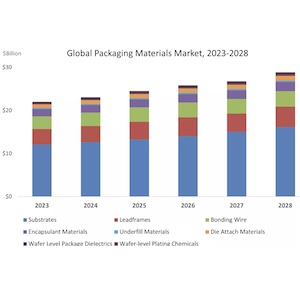
Powered by strong semiconductor demand across diverse end applications, the global semiconductor packaging materials market is expected to start a growth cycle with a 5.6% compound annual growth rate (CAGR) projected through 2028, SEMI, TECHCET and TechSearch International announced in their latest Global Semiconductor Packaging Materials Outlook (GSPMO) report. The report highlights AI as an expected growth driver for advanced packaging applications, despite currently low unit volumes due to the newness of the market segment.
The GSPMO report provides comprehensive data and forecasts for substrates, leadframes, bonding wire, and additional advanced packaging materials.
“After a challenging 2023, which saw a 15.5% decline in the semiconductor packaging materials market, our latest report forecasts a return to growth in 2024,” said Lita Shon-Roy, TECHCET President and CEO. “The global packaging materials market is expected to exceed $26 billion by 2025 and continue solid growth through 2028.”
Global packaging materials
“Substrates account for a large portion of the revenue for the packaging materials market, and within the category, FC-BGA substrates make up the majority of the revenue growth,” said Jan Vardaman, President of TechSearch International. “The CAGR for flip chip BGA/LGA revenue is expected to be 7.6% from 2023 to 2028. Other key growth areas include wafer-level packaging (WLP) dielectrics and flip chip underfill. The laminate substrates segment is expected to grow 7.3% annually in volume, while leadframes and bonding wire are also forecasted to recover, growing by 5.0% and 6.4%, respectively.”
The GSPMO 2024 report is designed to help companies capitalize on emerging trends, navigate supply chain challenges, and make informed decisions in sourcing high-performance materials.
Share on:


Testimonial
"In a year when every marketing dollar mattered, I chose to keep I-Connect007 in our 2025 plan. Their commitment to high-quality, insightful content aligns with Koh Young’s values and helps readers navigate a changing industry. "
Brent Fischthal - Koh YoungSuggested Items
Advanced Semiconductor Packaging Market Sees Rising Adoption Across Automotive and Industrial Sectors
10/14/2025 | openPRThe semiconductor packaging market size is estimated to reach at a CAGR of 7.2% during the forecast period (2024-2031).
Interposers, Substrates, and Advanced Manufacturing
10/13/2025 | Marcy LaRont, I-Connect007I attend a lot of industry trade shows and conferences. Lately, during conversations with technologists, I’ve noticed that there is some confusion about what exactly constitutes an interposer. One question I hear every so often is, “Are all interposers substrates?” The short answer to that question is no. But some interposers are, in fact, full substrates.
I-Connect007 Editor’s Choice: Five Must-Reads for the Week
10/10/2025 | Nolan Johnson, I-Connect007I-Connect007 has a new monthly digest newsletter, the Advanced Electronic Packaging Digest, and as I was scanning our advanced packaging newsfeeds this week, I came across a primer from tokenring.ai (republished through station WRAL, Raleigh, North Carolina), which I found quite useful. Whether you’re a designer, fabricator, or assembler, the package schemes being developed will change how you work, so be sure to keep your eye on the technological horizon and subscribe to the monthly Advanced Electronic Packaging Digest.
The Latest Issue: Advanced Electronics Packaging Digest to Explore Critical Minerals, Substrates, and Reliability Standards Driving Next-Gen Electronics
10/09/2025 | I-Connect007I-Connect007 is pleased to announce the upcoming issue of Advanced Electronics Packaging Digest (AEPD) on October 13, 2025, featuring expert insights on the technologies shaping the future of advanced packaging. As the electronics industry evolves, this issue takes a closer look at the materials, designs, and standards redefining performance and reliability across global markets.
Circular Packaging Market to Reach $98.0 Billion by 2035
10/08/2025 | Fact.MRThe market's journey from USD 45.8 billion in 2025 to USD 98.0 billion by 2035 represents substantial growth, the market will rise at a CAGR of 7.9% demonstrating the accelerating adoption of sustainable packaging systems and circular economy solutions across food & beverage, personal care, and e-commerce sectors.