


 Standard of Excellence: Speed vs. Quality in Customer Service
 Knocking Down the Bone Pile: Revamp Your Components with BGA Reballing
 Global Sourcing Spotlight: Balancing Speed and Flexibility Without Sacrificing Control


Keysight Unveils 3kV High Voltage Wafer Test System for Power Semiconductors
October 10, 2024 | BUSINESS WIREEstimated reading time: 1 minute
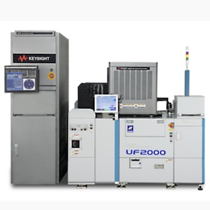
Keysight Technologies, Inc. introduces a 4881HV High Voltage Wafer Test System expanding its semiconductor test portfolio. The solution improves the productivity of power semiconductor manufacturers by enabling parametric tests up to 3kV supporting high and low-voltage in one-pass test.
Manufacturers have traditionally measured wafers using separate testers for high and low voltages. However, demand for power semiconductors is rapidly growing due to their multifunctionality, higher performance, and next-generation devices such as silicon carbide (SiC) and gallium nitride (GaN). As a result, customers need a solution to more accurately and efficiently test their devices and reduce time to market.
Keysight’s solution addresses these challenges by allowing power device makers to perform process control monitoring (PCM) and wafer acceptance testing (WAT) in manufacturing. The new test system delivers the following benefits:
High-Voltage Capability to Meet Future Needs: The high-voltage switching matrix (HV-SWM) supports up to 3kV requirements, is scalable up to 29 pins, and integrates with precision source measure units (SMUs). It enables highly flexible measurements from low current down to sub-pA resolution up to 3kV at any pins. Additionally, high-voltage capacitance measurement and various parametric tests are supported.
One-pass Testing Increases Productivity and Efficiency: The HV-SWM enables a single test system instead of separate high-voltage and low-voltage test systems. Utilizing one system is more efficient and reduces the required footprint and testing time. The system integrates with factory automation environments using Keysight’s SPECS-FA software, which improves the efficiency of the entire production process.
Enhanced Safety and Reliability: The test system has built-in protection circuitry and machine control, ensuring operators and equipment are not impacted by high-voltage surges during a test, and is compliant with safety regulations, including SEMI S2 standards.
Shinji Terasawa, Vice President and General Manager of Keysight's Wafer Test Solutions, said: “Keysight is thrilled to introduce our new wafer test system for power semiconductors, building on our long tenure of testing advanced semiconductors. Our mission is to lead the market by providing cutting-edge solutions that anticipate and meet the rapidly evolving needs of the semiconductor sector. This latest innovation exemplifies our unwavering commitment to the industry.”
Share on:


Testimonial
"Our marketing partnership with I-Connect007 is already delivering. Just a day after our press release went live, we received a direct inquiry about our updated products!"
Rachael Temple - AlltematedSuggested Items
TTCI Brings Hands-On Test Engineering and IPC Training Expertise to PCB Carolina 2025
10/31/2025 | The Test Connection Inc.The Test Connection Inc. (TTCI), a trusted provider of electronic test and manufacturing solutions, and The Training Connection LLC (TTC-LLC) will exhibit at PCB Carolina on Wednesday, November 12, 2025, at the McKimmon Center at NC State University in Raleigh, North Carolina. Attendees can visit Table 4 to say hello to Bert Horner and Bill Graver, and learn more about their test engineering services and technical training programs.
GEN3 Systems to Showcase Advanced Reliability Test Solutions at productronica 2025 in Munich
10/29/2025 | Gen3 SystemsGEN3 a leader in innovative reliability test solutions, is excited to announce its participation at productronica 2025, the world’s premier trade fair for electronics development and production.
Unlocking the Promise of AI in Electronics Manufacturing
10/29/2025 | Shobhit Agrawal, Keysight TechnologiesThe electronics manufacturing industry is rapidly evolving as more complicated products are introduced in the production lines, which require technological advancements even in the production processes. The requirements for production that is efficient, product quality that is greater, and product life cycles that are shorter are more crucial than ever before. In the electronic device life cycle, from design to maintenance, test phases have a significant impact on the economy of the company. Test processes are closely linked to the production volume and impacted by the complexity of the product. For businesses to maintain their competitive edge, they need to adopt innovative solutions and redefine processes.
New Episode of Voices of the Industry Podcast Explores Breakthroughs in Test and Inspection
10/22/2025 | I-Connect007In this episode of Voices of the Industry, “Testing Innovation: Advances in Test, Inspection & Failure Analysis,” host Nolan Johnson speaks with Rob Boguski, president of Datest. Together, they explore the expanding world of circuit testing, inspection, and failure analysis, areas that are experiencing a surge in technological capability and sophistication. As Johnson and Boguski discuss, today’s test companies are performing analyses and precision methods that would have seemed impossible just a decade ago.
HT Global Circuits Adds Two atg Luther & Maelzer Flying Probe Test Systems
10/15/2025 | atg Luther & Maelzer GmbHAtg Luther & Maelzer GmbH, a leading supplier of electrical testing solutions for the PCB industry, and IEC USA, a distributor of consumables, equipment, and services in the North American PCB market, confirm the order for high-speed bare board testing technology.