-

- News
- Books
Featured Books
- smt007 Magazine
Latest Issues
Current Issue
The Path Ahead
What are you paying the most attention to as we enter 2025? Find out what we learned when we asked that question. Join us as we explore five main themes in the new year.

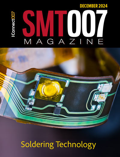
Soldering Technologies
Soldering is the heartbeat of assembly, and new developments are taking place to match the rest of the innovation in electronics. There are tried-and-true technologies for soldering. But new challenges in packaging, materials, and sustainability may be putting this key step in flux.

The Rise of Data
Analytics is a given in this industry, but the threshold is changing. If you think you're too small to invest in analytics, you may need to reconsider. So how do you do analytics better? What are the new tools, and how do you get started?
- Articles
- Columns
Search Console
- Links
- Media kit
||| MENU - smt007 Magazine
Keysight Collaborates with Siemens EDA to Enable the Next Generation of Wireless Design
October 23, 2024 | Keysight TechnologiesEstimated reading time: 1 minute
Keysight Technologies, Inc. and Siemens EDA have teamed up to accelerate the efficiency of wireless and defense system design. The integration between Keysight’s Advanced Design System (ADS) and the Siemens Xpedition Enterprise suite of EDA tools enables engineers to more efficiently co-design digital systems and radio frequency (RF) circuits by performing layout and manufacturing in Xpedition and RF Circuit and electromagnetic simulation in Keysight ADS.
Today’s complex wireless and defense system designs demand unprecedented levels of integration between RF and overall system design. These advanced solutions often combine intricate RF components, high-speed digital circuits, and sophisticated signal processing, all of which must work harmoniously.
The collaboration builds on the prior dynamic inter-tool integration from Keysight and Siemens EDA that enabled system design to have bidirectional integration with RF and microwave engineering tools. This initiative integrates complete hierarchical designs bidirectionally between Keysight ADS and Siemens Xpedition Designer and Layout, eliminating the cumbersome and error-prone task of manually translating libraries between the tools.
Engineers can now seamlessly transition between detailed RF design in ADS and system-level design in Xpedition, maintaining integrity across the entire development process. This is crucial for optimizing performance in areas including 5G/6G communications, advanced radar systems, and electronic warfare applications, where the interplay between RF and digital domains is critical to system performance.
The new product is included in Keysight Advanced Design System 2025 and Siemens Xpedition Enterprise release 2409.
Nilesh Kamdar, EDA Design & Verification lead at Keysight said:“We have a long-established track record collaborating with Siemens to support customers in enabling the next generation of wireless design. The bidirectional integration allows engineers to optimize performance across various applications, including 5G/6G and radar systems.”
AJ Incorvaia, Senior Vice President, Electronic Board Systems, Siemens Digital Industries Software said: “As engineering teams strive to achieve digital transformation, the digital thread between RF and electronic system design becomes more critical. We’re pleased to announce improved integration enabling concurrent design to optimize system performance and improve quality while accelerating design closure.”
Suggested Items
SMTA Hosts Ultra High Density Interconnect Symposium
12/31/2024 | SMTAThe Surface Mount Technology Association (SMTA) is pleased to announce the Ultra High Density Interconnect (UHDI) Symposium, taking place on Thursday, January 23 2025, at the Peoria Sports Complex in Peoria, Arizona.
IPC: PCB Designers Invited to Attend PEDC-Pan-European Electronics Design Conference
12/30/2024 | IPCThe Pan-European Electronics Design Conference (PEDC), co-hosted by FED and IPC, will take place on January 29-30, 2025.. This two-day conference, held in English, will bring together global PCB designers for a comprehensive exchange of ideas and insights on the latest trends and technologies in electronics design.
SP Manufacturing Expands with New Malaysia Plant, Acquires Ideal Jacobs
12/26/2024 | PRNewswireSP Manufacturing (SPM), a leader in Electronic Manufacturing Services (EMS), is strengthening its global presence with two major moves: opening a new manufacturing facility in Senai, Malaysia, and successfully acquiring Ideal Jacobs Corporation.
Robosys, ACUA Ocean + OREC Secure Funding For Collaborative Autonomy Project
12/25/2024 | RobosysAdvanced maritime autonomy developer, Robosys Automation, supported by USV manufacturer, ACUA Ocean, and Offshore Renewable Energy Catapult (OREC), have jointly secured grant funding through Innovate UK.
IPC Announces New Training Course: PCB Design for Military & Aerospace Applications
12/23/2024 | IPCIPC announced the launch of a new training course: PCB Design for Military & Aerospace Applications.


