-

- News
- Books
Featured Books
- smt007 Magazine
Latest Issues
Current Issue
Spotlight on Mexico
Mexico isn’t just part of the electronics manufacturing conversation—it’s leading it. From growing investments to cross-border collaborations, Mexico is fast becoming the center of electronics in North America. This issue includes bilingual content, with all feature articles available in both English and Spanish.

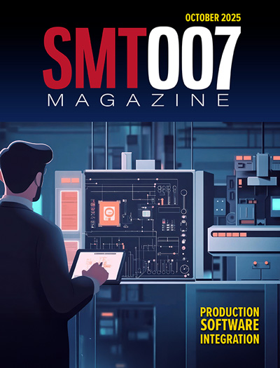
Production Software Integration
EMS companies need advanced software systems to thrive and compete. But these systems require significant effort to integrate and deploy. What is the reality, and how can we make it easier for everyone?

Spotlight on India
We invite you on a virtual tour of India’s thriving ecosystem, guided by the Global Electronics Association’s India office staff, who share their insights into the region’s growth and opportunities.
- Articles
Article Highlights
- Columns
- Links
- Media kit
||| MENU - smt007 Magazine
HBM5 20hi Stack to Adopt Hybrid Bonding Technology, Potentially Transforming Business Models
October 30, 2024 | TrendForceEstimated reading time: 1 minute
TrendForce reports that the focus on HBM products in the DRAM industry is increasingly turning attention toward advanced packaging technologies like hybrid bonding. Major HBM manufacturers are considering whether to adopt hybrid bonding for HBM4 16hi stack products but have confirmed plans to implement this technology in the HBM5 20hi stack generation.
Hybrid bonding offers several advantages when compared to the more widely used micro-bumping. Since it does not require bumps, it allows for more stacked layers and can accommodate thicker chips that help address warpage. Hybrid-bonded chips also benefit from faster data transmission and improved heat dissipation.
TrendForce indicates that the three major manufacturers will continue to use Advanced MR-MUF and TC-NCF stacking architectures for the HBM3e 12hi stack and HBM4 12hi stack. Meanwhile, a clear preference for the HBM4 16hi stack and HBM4e 16hi stack has yet to emerge between hybrid bonding and micro-bumping as hybrid bonding currently lacks significant advantages over micro-bumping.
If manufacturers opt for hybrid bonding, it would likely be to master the learning curve of this new stacking technology early to ensure smoother mass production of HBM4e and HBM5 products in the future. Manufacturers have confirmed that hybrid bonding will be used in the HBM5 20hi stack generation after taking into consideration limitations on stack height, IO density, and thermal management.
However, hybrid bonding comes with several challenges. For instance, manufacturers investing in new equipment to introduce the technology would reduce their reliance on micro-bumping, thereby losing any accumulated advantages in that area.
Hybrid bonding also presents technical challenges—such as particle control—which could drive up unit investment costs. Additionally, hybrid bonding requires wafer-to-wafer stacking, which could lead to inefficiencies if front-end production yields are too low and make overall production economically unfeasible.
TrendForce notes that the adoption of hybrid bonding could lead to significant shifts in the HBM business model. It becomes critical to ensure that the base die and memory die have identical chip dimensions with wafer-to-wafer stacking. Since the design of the base die is primarily handled by GPU/ASIC companies, TSMC, which offers both base die and GPU/ASIC foundry services, could take on the responsibility of stacking the base die and memory die. Should this development occur, it could significantly impact HBM manufacturers’ role in base die design, stacking, and overall HBM order management—potentially reshaping the competitive landscape.
Testimonial
"Our marketing partnership with I-Connect007 is already delivering. Just a day after our press release went live, we received a direct inquiry about our updated products!"
Rachael Temple - AlltematedSuggested Items
EV Group Achieves Breakthrough in Hybrid Bonding Overlay Control for Chiplet Integration
09/12/2025 | EV GroupEV Group (EVG), a leading provider of innovative process solutions and expertise serving leading-edge and future semiconductor designs and chip integration schemes, today unveiled the EVG®40 D2W—the first dedicated die-to-wafer overlay metrology platform to deliver 100 percent die overlay measurement on 300-mm wafers at high precision and speeds needed for production environments. With up to 15X higher throughput than EVG’s industry benchmark EVG®40 NT2 system designed for hybrid wafer bonding metrology, the new EVG40 D2W enables chipmakers to verify die placement accuracy and take rapid corrective action, improving process control and yield in high-volume manufacturing (HVM).
Indium Corporation Expert to Present on Automotive and Industrial Solder Bonding Solutions at Global Electronics Association Workshop
06/26/2025 | IndiumIndium Corporation Principal Engineer, Advanced Materials, Andy Mackie, Ph.D., MSc, will deliver a technical presentation on innovative solder bonding solutions for automotive and industrial applications at the Global Electronics A
OKI, NTT Innovative Devices Establish Mass Production Technology for High-Power Terahertz Devices by Heterogeneous Material Bonding
06/21/2025 | BUSINESS WIREOKI, in collaboration with NTT Innovative Devices Corporation, has established mass production technology for high-power terahertz devices using crystal film bonding (CFB) technology for heterogeneous material bonding to bond indium phosphide (InP)-based uni-traveling carrier photodiodes (UTC-PD) onto silicon carbide (SiC) with excellent heat dissipation characteristics for improved bonding yields.
See TopLine’s Next Gen Braided Solder Column Technology at SPACE TECH EXPO 2025
05/28/2025 | TopLineAerospace and Defense applications in demanding environments have a solution now in TopLine’s Braided Solder Columns, which can withstand the rigors of deep space cold and cryogenic environments.
Microsembly Furthers RF Hybrid Manufacturing Services with New Automated Wire Bonding and Die Attach Equipment
05/30/2025 | MicrosemblyMicrosembly, a US-based provider of high-frequency contract manufacturing services, has announced the addition of new state-of-the-art automated and manual wire and ribbon bonders to its advanced RF and microwave assembly, manufacturing, and testing facility.


