


 Standard of Excellence: The Future of Fabrication—From Art to Automation
 Knocking Down the Bone Pile: The Business Case for Component Reclamation
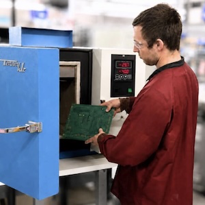
 Global Sourcing Spotlight: The Hidden Power of the Rep Network


When soldering electronic assemblies, the focus of the vacuum application is on the removal of volatile substances from the solder joints and the associated reduction of pore formation. Particularly in the thermal management of power electronics components, pores can cause so-called hotspots with higher temperatures due to their poor heat conduction. These hotspots can lead to overheating of the components on the one hand and to thermally induced destruction of the solder structure on the other. Vacuum soldering is used in the production of assemblies in the field of power electronics (e.g., inverters for electric cars and renewable energy sources).
Figure 1 shows various SMD components after soldering with and without vacuum. A comparison shows that with a vacuum of 10 mbar, both the number of pores and the pore area can be drastically minimized. In the case of flat solder joints, such as QFNs or Si chips, a low proportion of pores results in better thermal performance as well as less tilting of the component.
Figure 1: X-ray images of various SMD components after soldering without vacuum and with 10 mbar vacuum.
In addition to temperature profiling, the negative pressure in the vacuum chamber and the duration of the negative pressure are also set during vacuum soldering. Figure 2 shows the influence of these parameters on the proportion of pore area in the thermal pad of a QFN64 component.
Figure 2: X-ray images of the QFN64 solder joint after soldering without vacuum and after soldering at different vacuum levels and different holding times.
Previous experience from industry and research has led to the essential realization that pore formation depends on many factors and that a sustainable reduction of pores in the solder joints can only be achieved with the help of a vacuum process. A vacuum of 150 mbar can already reduce the proportion of pores from, for example, 40% to less than 10%. If very low void ratios (< 5%) are to be achieved, other parameters, such as the surface finish, the solder paste type, or the design of the pads, must also be considered. In addition to the primary goal of reducing porosity, vacuum soldering offers other advantages that vary depending on the soldering system. A comparison of the contact, condensation and convection soldering processes is presented below.
To continue reading this article, which originally published in the December 2024 edition of SMT007 Magazine, click here.


