ViTrox Welcomes Gemaddis as a New Sales Channel Partner in France
December 20, 2024 | ViTroxEstimated reading time: 1 minute

ViTrox Technologies, which aims to be the World’s Most Trusted Technology Company in delivering innovative, advanced, and cost-effective automated Machine Vision Inspection Solutions for the semiconductor and electronics manufacturing industries, is honoured to announce its partnership with Gemaddis as its new Sales Channel Partner (SCP) for the French market, effective May 2024.
This strategic collaboration marks another milestone in ViTrox’s commitment to expanding its footprint in the European market. As an authorised distributor, Gemaddis will offer ViTrox’s cutting-edge solutions across France, including the Advanced 3D Solder Paste Inspection (SPI) Solution, Advanced 3D Optical Inspection (AOI) Solution, Advanced 3D X-Ray Inspection (AXI) Solution, Advanced Robotic Vision (ARV) Solution, and Industry 4.0 Manufacturing Intelligence Solutions (V-ONE).
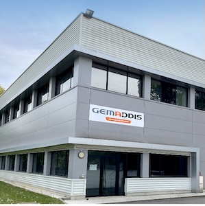
Gemaddis, a French company headquartered in Annecy, Haute-Savoie, was formed through the merger of GEMIDO and Addis Electronic. The company specialises in three key areas: the distribution of machines for the electronics industry, the design of solutions for electronics manufacturing, particularly for printed circuit assembly and process characterisation/ optimisation.
“Gemaddis is a well-established company with over 20 years of experience and substantial resources to support the regions they serve. Their expertise and strong market presence make them an excellent partner for ViTrox as we continue to expand our footprint in the European market,” said Mr Seow Zi Yang, Director of Business Development & Technical Support.
Testimonial
"In a year when every marketing dollar mattered, I chose to keep I-Connect007 in our 2025 plan. Their commitment to high-quality, insightful content aligns with Koh Young’s values and helps readers navigate a changing industry. "
Brent Fischthal - Koh YoungSuggested Items
Marcy’s Musings: Advancing the Advanced Materials Discussion
09/17/2025 | Marcy LaRont -- Column: Marcy's MusingsAs the industry’s most trusted global source of original content about the electronics supply chain, we continually ask you about your concerns, what you care about, and what you most want to learn about. Your responses are insightful and valuable. Thank you for caring enough to provide useful feedback and engage in dialogue.
Staying on Top of Signal Integrity Challenges
09/16/2025 | Andy Shaughnessy, Design007 MagazineOver the years, Kris Moyer has taught a variety of advanced PCB design classes, both online IPC courses and in-person classes at California State University-Sacramento, where he earned his degrees in electrical engineering. Much of his advanced curriculum focuses on signal integrity, so we asked Kris to discuss the trends he’s seeing in signal integrity today, the SI challenges facing PCB designers, and his go-to techniques for controlling or completely eliminating SI problems.
I-Connect007 Launches Advanced Electronics Packaging Digest
09/15/2025 | I-Connect007I-Connect007 is pleased to announce the launch of Advanced Electronics Packaging Digest (AEPD), a new monthly digital newsletter dedicated to one of the most critical and rapidly evolving areas of electronics manufacturing: advanced packaging at the interconnect level.
U.S. CHIPS Act Funding Detailed on SIA Website
09/12/2025 | Nolan Johnson, I-Connect007The U.S. CHIPS Act has moved well into the implementation stage in 2025. But where has that money gone? The Semiconductor Industry Association has been tracking these projects and provides details on its website. It was updated May. Among the five key programs being managed under CHIPS, two stand out as influencing advanced electronic packaging: the National Advanced Packaging Manufacturing Program (NAPMP), and the CHIPS Manufacturing USA Institute (MFG USA).
Advanced Packaging: Preparation is Now
09/15/2025 | Nolan Johnson, I-Connect007In this interview, Matt Kelly, CTO for the Global Electronics Association, and Devan Iyer, chief strategist of advanced packaging, define advanced electronics packaging and the critical nature of getting it right in the electronics manufacturing field. They share details from their white paper, “Advanced Packaging to Board Level Integration—Needs and Challenges,” and provide insight into how next-generation packaging will change the design, fabrication, and assembly of printed circuit boards, including the implications for final system assembly.