


 Dan’s Biz Bookshelf: ‘Atomic Habits’
 Happy’s Tech Talk #48: Digital Twins—Integrating Design and Manufacturing
 The Chemical Connection: The Consequences of Additive Metallizing on Etching Steps


The semiconductor industry is expected to start 18 new fab construction projects in 2025*, according to SEMI’s latest quarterly World Fab Forecast report. The new projects include three 200mm and fifteen 300mm facilities, the majority of which are expected to begin operations from 2026 to 2027.
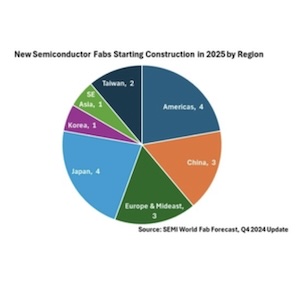
In 2025, the Americas and Japan are the leading regions with four projects each. The China and Europe & Middle East regions are each tied for third place with three planned construction projects. Taiwan has two planned projects, while Korea and Southeast Asia have one project each for 2025.
“The semiconductor industry has reached a pivotal juncture, with investments driving both leading-edge and mainstream technologies to meet evolving global demands,” said Ajit Manocha, SEMI President and CEO. “Generative AI and high-performance computing are fueling advancements in the leading-edge logic and memory segments, while mainstream nodes continue to underpin critical applications in automotive, IoT and power electronics. The construction of 18 new semiconductor fabs set to begin in 2025 demonstrates the industry’s commitment to support innovation and significant economic growth.”
Covering 2023 to 2025, the 4Q 2024 edition of World Fab Forecast report shows that the global semiconductor industry plans to begin operation of 97 new high-volume fabs. This includes 48 projects in 2024 and 32 projects set to launch in 2025, with wafer sizes ranging from 300mm to 50mm.
Advanced Nodes Lead Semiconductor Industry Expansion
Semiconductor capacity is projected to further accelerate, with a 6.6% yearly growth rate forecast to total 33.6 million wafers per month (wpm)** for 2025. This expansion will be primarily driven by leading-edge logic technologies in high-performance computing (HPC) applications and the increasing penetration of generative AI in edge devices.
The semiconductor industry is intensifying efforts to build advanced computing capabilities, responding to the escalating computational demands of large language models (LLMs). Chip manufacturers are aggressively expanding advanced node capacities (7nm and below), which are expected to see an industry-leading 16% yearly growth rate for an increase of more than 300,000 wpm to total 2.2 million wpm in 2025.
Boosted by China’s chip self-sufficiency strategy and expected demand from automotive and IoT applications, mainstream nodes (8nm~45nm) are predicted to add another 6% capacity, surpassing the 15 million wpm milestone in 2025.
Mature technology nodes (50nm and above) are experiencing a more conservative expansion, reflecting the market’s slow recovery and low utilization rates. This segment is expected to grow 5%, reaching 14 million wpm in 2025.
Foundry Segment Continues Strong Capacity Growth
Foundry suppliers are expected to remain the leaders in semiconductor equipment purchases. The Foundry segment is projected to increase capacity by 10.9% year-over-year, rising from 11.3 million wpm in 2024 to a record 12.6 million wpm in 2025.
The overall memory segment shows a measured capacity expansion, with modest growth of 3.5% in 2024 and 2.9% in 2025. However, strong generative AI demand is driving significant changes in memory markets. High-bandwidth memory (HBM) is experiencing a notable surge, creating divergent capacity growth trends between the DRAM and NAND flash segments.
The DRAM segment is expected to maintain robust growth, projecting approximately a 7% year-over-year increase to 4.5 million wpm in 2025. Conversely, the installed capacity for 3D NAND is anticipated to grow 5%, reaching 3.7 million wpm in the same period.
The latest update of the SEMI World Fab Forecast report, published in December 2024, lists more than 1,500 facilities and lines globally, including 180 volume facilities and lines with various probabilities expected to start operation in 2025 or later.


