-

- News
- Books
Featured Books
- smt007 Magazine
Latest Issues
Current Issue
Moving Forward With Confidence
In this issue, we focus on sales and quoting, workforce training, new IPC leadership in the U.S. and Canada, the effects of tariffs, CFX standards, and much more—all designed to provide perspective as you move through the cloud bank of today's shifting economic market.

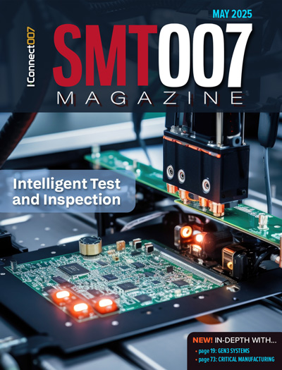
Intelligent Test and Inspection
Are you ready to explore the cutting-edge advancements shaping the electronics manufacturing industry? The May 2025 issue of SMT007 Magazine is packed with insights, innovations, and expert perspectives that you won’t want to miss.

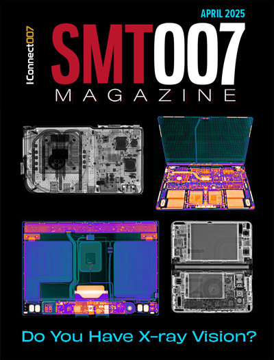
Do You Have X-ray Vision?
Has X-ray’s time finally come in electronics manufacturing? Join us in this issue of SMT007 Magazine, where we answer this question and others to bring more efficiency to your bottom line.
- Articles
- Columns
Search Console
- Links
- Media kit
||| MENU - smt007 Magazine
Micron Breaks Ground on New HBM Advanced Packaging Facility in Singapore
January 10, 2025 | MicronEstimated reading time: 2 minutes
Micron Technology, Inc. broke ground today on a new High-Bandwidth Memory (HBM) advanced packaging facility adjacent to the company’s current facilities in Singapore. Micron marked the occasion with a ceremony attended by Gan Kim Yong, Deputy Prime Minister and Minister for Trade and Industry of Singapore, Png Cheong Boon, Chairman of the Singapore Economic Development Board, Pee Beng Kong, Executive Vice President of the Singapore Economic Development Board, and Tan Boon Khai, CEO of JTC Corporation.
The new HBM advanced packaging facility will be the first facility of its kind in Singapore. Operations for the new facility are scheduled to begin in 2026, with meaningful expansion of Micron’s total advanced packaging capacity beginning in calendar 2027 to meet the demands of AI growth. The launch of this facility will further strengthen Singapore’s local semiconductor ecosystem and innovation.
“As AI adoption proliferates across industries, the demand for advanced memory and storage solutions will continue to increase robustly,” said Sanjay Mehrotra, president and CEO of Micron. “With the continued support of the Singapore government, our investment in this HBM advanced packaging facility strengthens our position to address the expanding AI opportunities ahead.”
Micron’s HBM advanced packaging investment of approximately US $7 billion (SG$9.5 billion) through the end of the decade and beyond will initially create around 1,400 jobs, with site expansion plans to reach an estimated 3,000 jobs in the future. These new roles will include functions such as packaging development, assembly and test operations.
Png Cheong Boon, Chairman of the Singapore Economic Development Board, said, “We welcome this significant investment by Micron, which reflects its confidence in Singapore’s competitiveness as a critical node in the global semiconductor supply chain. This is Singapore’s first high-bandwidth memory advanced packaging facility, allowing us to contribute to global AI growth. It expands Singapore’s partnership with Micron and further strengthens the semiconductor ecosystem in Singapore.”
Micron’s future expansion plans in Singapore will also support long-term manufacturing requirements for NAND.
Micron will maintain flexibility in managing the pace of capacity ramps in both the HBM and NAND facilities to align with market demand.
Micron’s current facility in Singapore is the first front-end semiconductor fab in the world to be recognized as the Advanced Fourth Industrial Revolution Lighthouse and Sustainability Lighthouse by the World Economic Forum. The new HBM advanced packaging facility will be built in alignment with Micron’s sustainability commitments. It will feature technologies such as a greenhouse gas abatement, water recycling and waste circularity (reduce, reuse, recycle, recover). The new building will be highly automated through AI-based intelligent solutions and designed to meet the Leadership in Energy and Environmental Design (LEED) certification requirements.
Suggested Items
New Era Electronics Establishes U.S. Presence with New Salt Lake City Operation
06/04/2025 | PRNewswireNew Era Electronics, a leading provider of high-performance industrial computing solutions, announces the establishment of its first United States location in Salt Lake City, Utah. This strategic expansion to the U.S. underscores New Era Electronics' commitment to enhancing supply chain continuity and delivering exceptional services across North America.
Elma Electronic Bolsters Quality Management Company-wide with Added AS9100:D and ISO9001:2015 Certifications
06/02/2025 | Elma ElectronicElma Electronic now includes AS9100:D and ISO 9001:2015 certifications at its Horsham, Pa. manufacturing facility, earning the company a multiple site accreditation designation.
atg Luther Maelzer Announces Grand Opening of New Office and Manufacturing Facility
06/02/2025 | atg Luther & Maelzer GmbHAtg Luther Maelzer, a leading supplier of electrical testing solutions for the PCB industry, recently celebrated with a grand opening of their new office and manufacturing facility in Wertheim, Germany.
Kimball Electronics to Open New Medical Manufacturing Facility
05/30/2025 | Kimball ElectronicsKimball Electronics has announced the addition of a 300,000 sq ft manufacturing facility in Indianapolis centered on the medical industry.
MKS Opens New State-of-the-Art Facility in Derio, Spain to Strengthen Iberian and Southern European Presence
05/28/2025 | MKS’ AtotechMKS’ Atotech, a leading surface finishing brand of MKS Instruments, proudly announces the official opening of its new facility in Derio, Bizkaia, Spain, a strategic investment designed to support the company’s General Metal Finishing business across the Iberia Region, including Spain and Portugal.


