-
- News
- Books
Featured Books
- smt007 Magazine
Latest Issues
Current Issue
Spotlight on North America
A North America spotlight exploring tariffs, reshoring, AI demand, and supply chain challenges. Plus, insights on cybersecurity, workforce development, and the evolving role of U.S. electronics manufacturing.
Wire Harness Solutions
Explore what’s shaping wire harness manufacturing, and how new solutions are helping companies streamline operations and better support EMS providers. Take a closer look at what’s driving the shift.
Spotlight on Europe
As Europe’s defense priorities grow and supply chains are reassessed, industry and policymakers are pushing to rebuild regional capability. This issue explores how Europe is reshaping its electronics ecosystem for a more resilient future.
- Articles
- Columns
- Links
- Media kit
||| MENU - smt007 Magazine
Altus Enhances Traceability for Leading CEM
March 4, 2025 | Altus GroupEstimated reading time: 2 minutes
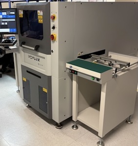
Altus Group, a leading supplier of capital equipment for the electronics industry, has helped Active PCB Solutions, a UK-based Contract Electronics Manufacturer, enhance its traceability with the installation of the YJ Link YLM Laser Marker. This investment supports the company’s commitment to delivering high-quality products to demanding sectors.
Active PCB sought to enhance productivity further by moving away from a manual, resource-intensive labelling process to enhance its traceability system. After evaluating several options, the company selected the YJ Link YLM Laser Marker from Altus Group due to its advanced features and seamless integration into their production process.
Jason Hancock, Head of Engineering at Active PCB Solutions, said: “With traceability and process improvements being key to delivering the highest quality to our customers, it was important to move away from a manual high-cost process. The YJ Link laser marker, supported by Altus, has provided an efficient and reliable solution.”
The YJ Link YLM Laser Marker stood out for its capability to automate the repetitive labelling process, increasing productivity and allowing staff to focus on more complex tasks. Its internal flip functionality enables double-sided PCB marking without manual intervention, streamlining workflow and reducing handling time. The system’s large working area accommodates a wide range of board sizes, enhancing production flexibility. Equipped with a high-quality Keyence laser head, the YLM delivers precise, high-contrast markings, ensuring accurate traceability throughout the product lifecycle.
Joe Booth, CEO of Altus Group, said: “Active PCB’s investment in the YJ Link Laser Marker highlights their commitment to operational efficiency and quality. We’re pleased to provide a solution that enhances productivity and offers exceptional value.”
Since its installation, the YJ Link YLM Laser Marker has optimised Active PCB’s production workflow and delivered cost savings by automating the labelling process. The precise and durable laser markings ensure consistent traceability, supporting Active PCB’s high-quality standards.
Testimonial
"The I-Connect007 team is outstanding—kind, responsive, and a true marketing partner. Their design team created fresh, eye-catching ads, and their editorial support polished our content to let our brand shine. Thank you all! "
Sweeney Ng - CEE PCBSuggested Items
LPKF Gets Off to a Solid Start in 2026
05/04/2026 | LPKFLPKF Laser & Electronics SE has made a solid start to the 2026 financial year despite a macroeconomic environment that remains challenging.
Driving Innovation: Selecting the Right Laser Source
04/28/2026 | Simon Khesin -- Column: Driving InnovationWhen I first joined Schmoll Maschinen, I brought experience from almost every PCB process, except for laser. As I immersed myself in laser processing, I realized why it can seem so daunting to a newcomer. The complexity arises from three intersecting factors: A vast variety of laser sources: CO2, UV-nano, green-pico, UV-pico, IR-pico, and others; a diverse range of applications: Drilling, cutting, ablation, and more; and an extensive list of materials: These have vastly different absorption rates. Choosing the right machine or laser source is rarely trivial. Even for experienced engineers, answering "Which source is best?" requires examining the business's specific goals.
AI, HDI, and Interconnect Optimization with MKS' ESI
04/23/2026 | Real Time with... APEX EXPOThis discussion revolves around the transformative impact of AI on HDI and substrate manufacturing. Casey Krueger explains the company's "Optimize the Interconnect" initiative, which features Atotech, to provide a comprehensive solution from pretreatment to laser drilling. MKS' ESI offers the innovative Geode G2 platform which is an advanced laser drilling technology that enhances productivity, reduces energy consumption, and addresses complex design challenges in processing both PCB and ICP materials.
Horizon Sales Adds LPKF Laser and Electronics to Its Lineup
04/21/2026 | Horizon SalesHorizon Sales, a leading manufacturers’ representative and distributor to the electronics industry, is pleased to announce a new partnership with LPKF Laser and Electronics, a global leader in precision laser technology
Future-proof Laser Depaneling for PCBs with Photonics
04/10/2026 | Real Time with... APEX EXPOBill Solari of Photonics Systems USA outlines the advantages of laser depaneling for circuit board manufacturing. We learn that this advanced technology addresses rising material costs by increasing panel yield and improving edge quality. This process provides precision, suitability for medical applications, and cost-saving benefits, including the elimination of cleaning steps. There have been significant advancements in laser depaneling, offering a competitive and efficient solution for modern electronics production.