-

- News
- Books
Featured Books
- design007 Magazine
Latest Issues
Current Issue
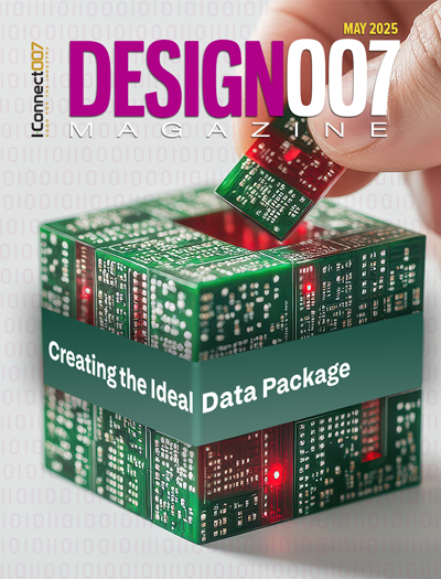
Creating the Ideal Data Package
Why is it so difficult to create the ideal data package? Many of these simple errors can be alleviated by paying attention to detail—and knowing what issues to look out for. So, this month, our experts weigh in on the best practices for creating the ideal design data package for your design.

Designing Through the Noise
Our experts discuss the constantly evolving world of RF design, including the many tradeoffs, material considerations, and design tips and techniques that designers and design engineers need to know to succeed in this high-frequency realm.

Learning to Speak ‘Fab’
Our expert contributors clear up many of the miscommunication problems between PCB designers and their fab and assembly stakeholders. As you will see, a little extra planning early in the design cycle can go a long way toward maintaining open lines of communication with the fab and assembly folks.
- Articles
- Columns
Search Console
- Links
- Media kit
||| MENU - design007 Magazine
Multicircuits Expands Capabilities with State-of-the-Art Automated Copper Via Fill Process
March 10, 2025 | MulticircuitsEstimated reading time: 1 minute
Mike Thiel, president of Multicircuits, a leading provider of high-reliability printed circuit boards, has announced the addition of a state-of-the-art automated copper via fill process to their advanced manufacturing capabilities. This strategic investment enhances the company’s ability to deliver cutting-edge solutions for demanding industries, including aerospace, defense, medical, and high-speed telecommunications.
Copper via fill technology plays a crucial role in improving signal integrity, increasing thermal conductivity, and enhancing circuit density. This advanced process ensures superior performance for high-density interconnect (HDI) and multilayer PCBs, reinforcing Multicircuits' reputation as an industry leader in precision manufacturing.
“We continuously invest in cutting-edge technologies to provide our customers with the most advanced PCB solutions,” said Mr. Thiel when making the announcement. “The addition of copper via fill strengthens our commitment to innovation and positions us as a premier partner for high-performance electronics manufacturing.”
Dave Kemper, Process Engineering Manager at Multicircuits, highlighted the technical advantages of this new capability, “This new process allows us to manufacture more robust PCBs with improved electrical and thermal properties. Our team has worked diligently to ensure a seamless integration of this process, and we are excited to offer this enhanced service to our customers.”
With the introduction of automated copper via fill, Multicircuits continues to push the boundaries of PCB technology, delivering superior reliability and performance to customers across a wide range of industries.
Suggested Items
Scanfil Boosts Investment in Electronics Manufacturing in the US
05/08/2025 | BUSINESS WIREScanfil is investing in a second electronics manufacturing line in Atlanta, Georgia, USA. The demand for manufacturing electronics in the USA has increased over the past two years and is expected to continue growing.
ZESTRON Announces New Reliability and Solutions Service for Risk Assessment & Mitigation of Electronic Assemblies
05/06/2025 | ZESTRONZESTRON, the leading global provider of high-precision cleaning products, services, and training solutions, is thrilled to introduce its new Reliability and Solutions (R&S) service.
Knocking Down the Bone Pile: Gold Mitigation for Class 2 Electronics
05/07/2025 | Nash Bell -- Column: Knocking Down the Bone PileIn electronic assemblies, the integrity of connections between components is paramount for ensuring reliability and performance. Gold embrittlement and dissolution are two critical phenomena that can compromise this integrity. Gold embrittlement occurs when gold diffuses into solder joints or alloys, resulting in mechanical brittleness and an increased susceptibility to cracking. Conversely, gold dissolution involves the melting away of gold into solder or metal matrices, potentially altering the electrical and mechanical properties of the joint.
Happy’s Tech Talk #38: Novel Metallization for UHDI
05/07/2025 | Happy Holden -- Column: Happy’s Tech TalkI have been involved in high-density electronics substrates since 1970 when I joined Hewlett-Packard’s RF semiconductor group after college. Figure 1 shows the difference between trace/space lithography for substrates and silicon starting in 1970. My projects involved sapphire circuits for RF devices, but the figure displays the state of PCBs and integrated CMOS circuits and their packaging, not discreet RF devices. Even then, semiconductors were 50X higher density.
Elma’s AI Optimized CompacFrame Speeds Development of Rugged GPU-focused Applications
05/05/2025 | Elma ElectronicElma Electronic has expanded its line of SOSA aligned CompacFrame development chassis to include an AI (artificial intelligence) optimized 7-slot version.


