Merlin Circuit Technology Invest in ESI 5335 Laser Drill Technology
March 19, 2025 | Merlin Circuit TechnologyEstimated reading time: Less than a minute

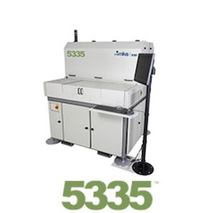
Merlin has been manufacturing HDI products for more than 15 years, firstly with mechanical drilled micro vias and subsequently laser drilled vias with an ESI 5330 Laser Drill. This is an established technology that has developed and increased in volume over the years, with the increase in demand for these products Merlin has invested in an ESI 5335 Laser Drill
The 5335 incorporates a high-power diode-pumped laser to enable efficient cutting through copper-clad laminates, with a range of parameters to deliver greater swarf / debris removal, thus achieving improved hole wall definition to aid subsequent plating processes and product reliability.
Improved productivity is also gained with operational speeds of up to three times faster than previously possible, the 5335 has a peak move speed of 14,000 points per second @ 250 µm spacing, greater accuracy +/- 20 um over the entire panel with holes down to 0.05um dia.
This is a fantastic investment for Merlin and demonstrates a continued commitment to invest in the technologies required to service a developing and demanding circuit board industry at the highest level.
Testimonial
"Our marketing partnership with I-Connect007 is already delivering. Just a day after our press release went live, we received a direct inquiry about our updated products!"
Rachael Temple - AlltematedSuggested Items
EV Group Achieves Breakthrough in Hybrid Bonding Overlay Control for Chiplet Integration
09/12/2025 | EV GroupEV Group (EVG), a leading provider of innovative process solutions and expertise serving leading-edge and future semiconductor designs and chip integration schemes, today unveiled the EVG®40 D2W—the first dedicated die-to-wafer overlay metrology platform to deliver 100 percent die overlay measurement on 300-mm wafers at high precision and speeds needed for production environments. With up to 15X higher throughput than EVG’s industry benchmark EVG®40 NT2 system designed for hybrid wafer bonding metrology, the new EVG40 D2W enables chipmakers to verify die placement accuracy and take rapid corrective action, improving process control and yield in high-volume manufacturing (HVM).
ROHM Develops Ultra-Compact CMOS Op Amp: Delivering Industry-Leading Ultra-Low Circuit Current
09/11/2025 | ROHMROHM’s ultra-compact CMOS Operational Amplifier (op amp) TLR1901GXZ achieves the industry’s lowest operating circuit current.
I-Connect007 Launches New Podcast Series on Ultra High Density Interconnect (UHDI)
09/16/2025 | I-Connect007I-Connect007 is excited to announce the debut of its latest On the Line With... podcast series, which shines a spotlight on one of the most important emerging innovations in electronics manufacturing: Ultra-High-Density Interconnect (UHDI).
I-Connect007 Launches New Podcast Series on Ultra High Density Interconnect (UHDI)
09/10/2025 | I-Connect007I-Connect007 is excited to announce the debut of its latest podcast series, which shines a spotlight on one of the most important emerging innovations in electronics manufacturing: Ultra-High-Density Interconnect (UHDI). The series kicks off with Episode One, “Ultra HDI: What does it mean to people? Why would they want it?” Host Nolan Johnson is joined by guest expert John Johnson, Director of Quality and Advanced Technology at American Standard Circuits (ASC).
KYZEN to Feature High-Reliability MICRONOX Chemistries at IMAPS Symposium
09/10/2025 | KYZEN'KYZEN, the global leader in innovative environmentally responsible cleaning chemistries, is pleased to announce its participation at the International Symposium on Microelectronics or IMAPS Symposium, taking place September 29-October 3 at Town & Country Resort in San Diego, CA.