


 It’s Only Common Sense: Just Imagine…
 Marcy’s Musings: Old School vs. New School—When Does It Matter?
 The Hidden Enabler of Autonomous Warfare: Advanced PCB Technologies Behind Defense AI


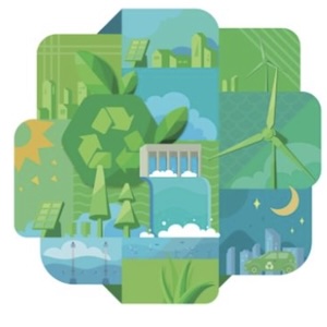
Conventional printed circuit board (PCB) manufacturing is wasteful, harmful to the environment and energy intensive. This can be mitigated by the implementation of new recyclable materials and technologies, which have the potential to revolutionize electronics manufacturing.
During research interviews for the report "Sustainable Electronics and Semiconductor Manufacturing 2025-2035: Players, Markets, Forecasts", IDTechEx found that recent research and testing developments have resulted in many of these materials approaching full-scale commercial readiness, whilst cost and performance remain a barrier for many others.
New substrates
FR4 remains the dominant substrate of choice for PCBs, a glass-reinforced epoxy resin laminate. It is lightweight, strong, and cheap. However, it is also non-recyclable and can contain toxic halogenated flame retardants, which can be released into the atmosphere at end-of-life through incineration. This makes alternative substrates desirable, which could be bio-based, biodegradable or recyclable.
One promising new material is JIVA's Soluboard®, a biodegradable substrate made from the natural fibers flax and jute. It dissolves in 90°C water, allowing component recycling and precious metal recovery at end of life. The substrate is currently being tested by companies such as Microsoft, Infineon, and Jaguar, who also see it as a method to combat rising global e-waste levels.
Polylactic acid is another sustainable material with opportunities in flexible PCBs. The chemical can be sourced from organic industrial waste and is also biodegradable. Conventional flexible PCBs are made from the plastic polyimide, with sustainably sourced alternatives yet to be found. Polylactic acid could be the solution, currently in the protype scale validation phase, demonstrated by companies and research institutes such as VTT. It can withstand temperatures of up to 140°C, which is lower than that of polyimide and FR4, but is compatible with manufacturing processes such as silver ink sintering.
Sustainable soldering
Mayerhofer Electronik was the first to demonstrate the use of second-life tin for soldering in its electronics manufacturing processes. 180,000 tonnes of primary tin are used in electronics globally, primarily sourced from mines in China, Indonesia and Myanmar, causing significant environmental damage. The quality of recycled tin is the same as primary tin, confirmed by X-ray diffraction. It is produced by smelting waste metal and metal oxide. Only around 30% of tin is currently recycled worldwide so there is huge potential for a push towards a circular economy in soldering processes.
Strong regulatory drivers are expected to encourage increased metal recycling, with secondary copper another with the potential for implementation into electronics. The strongest regulation so far is seen in Germany. Their National Circular Economy Strategy (NKWS) unveiled in 2024 aims to half per capita raw material consumption by 2045. It also aims to double the share of recycled materials across all industries and reduce municipal waste by 10%. Apple have committed to using secondary tin in all products by 2035. There is scope for more companies to follow suit or even implement secondary tin sooner.
Recovering copper waste and chemical etchants
Copper is used wastefully in PCBs. A flat sheet of copper is applied to the substrate, before holes are drilled and a circuit pattern produced by etching away the excess copper, which requires large volumes of chemical etchants such as ferric (III) chloride and cupric (II) chloride. Around 70% of the copper initially applied to the board is often removed.
One way of removing this waste of copper is to employ additive manufacturing, in which copper is only applied where it is required. Adoption of these techniques has been limited due to the capital costs of switching manufacturing methods. A method that requires no manufacturing switch is to employ etchant regeneration systems, which recover both copper that has been etched from the laminate, and etchant chemicals. This recycled copper can then serve as an additional revenue stream to the electronics manufacturer. These regeneration systems have been commercially available for over a decade and have been found to have a payback period of roughly 6 to 18 months. Systems are available using chlorine gas as an oxidizing agent or utilizing electrolysis. The latter has a larger energy requirement. Both can extend the lifetime of etchants. For ferric (III) chloride the lifetime is roughly tripled, and hydrochloric acid consumption can be reduced by around 95%.
Further sustainable electronics manufacturing insights
Increased recycling has the potential to significantly reduce material waste from electronics recycling, as well as potentially reducing energy requirements through less material production required. Recyclable and biodegradable materials also tend to be less harmful to the environment than some of the conventionally used materials. However, increasing the use of recyclable materials is just one way the sustainability of electronics manufacturing can be improved.


