


 Trouble in Your Tank: Understanding Interconnect Defects, Part 1
 It’s Only Common Sense: Marketing Isn’t Fluff, It’s Ammunition
 Driving Innovation: Mechanical and Optical Processes During Rigid-flex Production


Summit Interconnect Hollister Elevates PCB Prototyping with New TiTAN Direct Imaging System from Technica USA
May 1, 2025 | Summit Interconnect, Inc.Estimated reading time: 1 minute
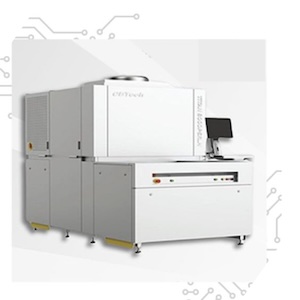
Summit Interconnect’s Hollister facility has recently enhanced its quick-turn PCB prototyping capabilities by installing the TiTAN PSR-H Direct Imaging (DI) system. This advanced equipment, developed by CBT and supplied by Technica USA, is renowned for its high-speed, high-resolution imaging capabilities, particularly for photoimageable solder masks.
The TiTAN PSR-H model offers several key features:
- High-Speed Imaging: Recognized as the fastest in its class for all photoimageable solder masks, including standard, black, and white variants.
- Versatility: Capable of handling both dry film and solder mask printing with exceptional front-to-back registration accuracy.
- Precision: Delivers print resolutions down to 10 microns, powered by CBT’s patented technology.
This installation aligns with Summit Interconnect’s commitment to integrating cutting-edge technology across its facilities to meet the evolving demands of the PCB industry. The Hollister site, known for specializing in 24-hour quick-turn PCB prototyping, will benefit from the TiTAN system’s capabilities, ensuring faster turnaround times and enhanced quality for complex PCB designs.
By investing in such advanced imaging technology, Summit Interconnect reinforces its position as a leading provider of high-reliability, advanced technology printed circuit boards in North America. This move not only boosts the Hollister facility’s operational efficiency but also enhances its ability to serve industries requiring rapid prototyping and precision manufacturing.
Share on:


Testimonial
"Advertising in PCB007 Magazine has been a great way to showcase our bare board testers to the right audience. The I-Connect007 team makes the process smooth and professional. We’re proud to be featured in such a trusted publication."
Klaus Koziol - atgSuggested Items
Green Circuits Appoints Kaitlyn Muhlenforth as Marketing Manager
11/05/2025 | Green CircuitsGreen Circuits, a full-service Electronics Manufacturing Services (EMS) partner to leading OEMs, is excited to announce the appointment of Kaitlyn Muhlenforth as its new Marketing Manager.
On the Line With… Ultra HDI, Episode 8: “Materials, Up and Coming Capabilities,” Now Available
11/05/2025 | I-Connect007I-Connect007 is excited to announce the release of the eighth episode of its 12-part podcast series, On the Line With… American Standard Circuits: Ultra HDI. In this episode, “Materials, Up and Coming Capabilities,” host Nolan Johnson sits down with resident expert John Johnson, Director of Quality and Advanced Technology at American Standard Circuits, to discuss how material selection influences the Ultra HDI (UHDI) manufacturing process.
Target Condition: Distribution of Power—Denounce the Ounce
11/05/2025 | Kelly Dack -- Column: Target ConditionHave you ever wondered why the PCB design segment uses ounces to describe copper thickness? There’s a story behind all of this—a story that’s old, dusty, and more than a little absurd. (Note that I didn’t add “Like many of us.”) Legend has it that back in the days of copper tinkers and roofing tradesmen, the standard was set when a craftsman hammered out a sheet of copper until it weighed one ounce, when its area conveniently matched the square of the king’s foot.
Henger Microelectronics Expands Global Footprint with Major Equipment Shipment to Southeast Asia
10/31/2025 |Henger Microelectronics has reached a major milestone in its global expansion strategy with the successful shipment of advanced plasma etching and cleaning systems, along with automation equipment, to multiple countries and regions across Southeast Asia. This achievement marks a significant step forward in the company’s international growth and reinforces its position as a leading force in the global plasma equipment industry.
I-Connect007 Editor’s Choice: Five Must-Reads for the Week
10/31/2025 | Nolan Johnson, I-Connect007Last week, the IMPACT conference took place in Taipei, bringing together advanced packaging experts from around the globe to share their knowledge. We’ll be bringing you post-conference coverage over the next few weeks, so look for that in our newsletters, and in the Advanced Electronic Packaging Digest. Other news seemed to have the U.S. at the center of the global discussions. My picks start in Phoenix, where TSMC, NVIDIA, and Amkor are all scrambling to establish new capabilities. There’s nothing like a strong demand signal to cause build-out, and AI chips are doing exactly that.