


 It’s Only Common Sense: If You’re Not Differentiated, You’re Dead
 Alpha Insights, Performance by Design: The Future of PCB Manufacturing in the Midwest
 Happy’s Tech Talk #43: Engineering Statistics Training With Free Software


Deca Announces Agreement with IBM to Bring High-Density Fan-Out Interposer Production to North America
May 20, 2025 | Deca TechnologiesEstimated reading time: 1 minute
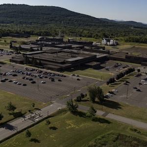
Deca Technologies announced the signing of an agreement with IBM to implement Deca’s M-Series™ and Adaptive Patterning® technologies in IBM’s advanced packaging facility in Bromont, Quebec. Through the agreement, IBM will implement a high-volume manufacturing line with a focus on Deca’s M-Series Fan-out Interposer Technology (MFIT™).
This collaboration builds on IBM’s strategy to develop its advanced packaging capabilities. IBM Canada's plant in Bromont is one of North America’s largest semiconductor assembly and test sites and has been at the forefront of packaging innovation for over five decades. Recent investments to expand the site’s capabilities have positioned it as a critical hub for high-performance packaging and chiplet integration, supporting technologies like MFIT that are essential for AI, HPC, and data center applications.
Deca’s M-Series platform is the highest-volume fan-out packaging technology in the world, with over seven billion M-Series units shipped. MFIT builds on this proven foundation by integrating embedded bridge die for chips’ last processor and memory integration delivering high-density, low-latency connections between chiplets. MFIT provides a cost-effective alternative to full silicon interposers, offering improved signal integrity, greater design flexibility, and the scalable format needed for ever-larger AI, HPC, and data center devices.
This cooperation reflects the shared commitment of IBM and Deca to advance the next generation of semiconductor packaging. By combining IBM’s advanced packaging capabilities with Deca’s proven technology, the two companies are expanding the global supply chain for the future of high-performance chiplet integration and advanced computing systems.
“Advanced packaging and chiplet technology are critical for faster, more efficient computing solutions in the age of AI. Deca will help ensure IBM’s Bromont facility remains at the forefront of these innovations, strengthening our commitment to helping our clients bring products to market faster and deliver better performance for AI and data-heavy applications,” said Scott Sikorski, Head of Business Development for Chiplets & Advanced Packaging at IBM.
“IBM’s rich history in semiconductor innovation and advanced packaging makes them an ideal partner to bring MFIT to high-volume production,” said Tim Olson, Founder and CEO of Deca. “We are thrilled to be working together to bring this advanced interposer technology to the North American ecosystem.”
Share on:


Testimonial
"The I-Connect007 team is outstanding—kind, responsive, and a true marketing partner. Their design team created fresh, eye-catching ads, and their editorial support polished our content to let our brand shine. Thank you all! "
Sweeney Ng - CEE PCBSuggested Items
Advanced Semiconductor Packaging Market Sees Rising Adoption Across Automotive and Industrial Sectors
10/14/2025 | openPRThe semiconductor packaging market size is estimated to reach at a CAGR of 7.2% during the forecast period (2024-2031).
Interposers, Substrates, and Advanced Manufacturing
10/13/2025 | Marcy LaRont, I-Connect007I attend a lot of industry trade shows and conferences. Lately, during conversations with technologists, I’ve noticed that there is some confusion about what exactly constitutes an interposer. One question I hear every so often is, “Are all interposers substrates?” The short answer to that question is no. But some interposers are, in fact, full substrates.
I-Connect007 Editor’s Choice: Five Must-Reads for the Week
10/10/2025 | Nolan Johnson, I-Connect007I-Connect007 has a new monthly digest newsletter, the Advanced Electronic Packaging Digest, and as I was scanning our advanced packaging newsfeeds this week, I came across a primer from tokenring.ai (republished through station WRAL, Raleigh, North Carolina), which I found quite useful. Whether you’re a designer, fabricator, or assembler, the package schemes being developed will change how you work, so be sure to keep your eye on the technological horizon and subscribe to the monthly Advanced Electronic Packaging Digest.
The Latest Issue: Advanced Electronics Packaging Digest to Explore Critical Minerals, Substrates, and Reliability Standards Driving Next-Gen Electronics
10/09/2025 | I-Connect007I-Connect007 is pleased to announce the upcoming issue of Advanced Electronics Packaging Digest (AEPD) on October 13, 2025, featuring expert insights on the technologies shaping the future of advanced packaging. As the electronics industry evolves, this issue takes a closer look at the materials, designs, and standards redefining performance and reliability across global markets.
Circular Packaging Market to Reach $98.0 Billion by 2035
10/08/2025 | Fact.MRThe market's journey from USD 45.8 billion in 2025 to USD 98.0 billion by 2035 represents substantial growth, the market will rise at a CAGR of 7.9% demonstrating the accelerating adoption of sustainable packaging systems and circular economy solutions across food & beverage, personal care, and e-commerce sectors.