Creating a Design Constraint Strategy
July 24, 2025 | I-Connect007 Editorial TeamEstimated reading time: 2 minutes
Feature Q&A With Kris Moyer, Global Electronics Association
Most designers learn how to set their design constraints through trial and error. EDA vendors’ guidelines explain how to use their particular tools’ constraints, and IPC standards offer a roadmap, but PCB designers usually develop their own unique styles for setting constraints.
Is there a set of best practices for setting constraints? That’s what I asked Global Electronics Association design instructor Kris Moyer, who covers design constraints in his classes. In this interview, Kris discusses how to identify PCB design requirements and set design constraints tightly enough for performance but flexible enough for manufacturing limitations.
What pre-layout analysis should be performed before you begin setting constraints?
Kris Moyer: There are several analyses that should be completed before setting constraints. These include the following:
- Timing/signal integrity: Used to set controlled impedance, termination, length matching and max length, and layer restrictions for digital signals.
- SPICE/power integrity analysis: Used to define the power distribution network (PDN) limits, the current requirements (trace widths), and voltage clearance requirements (Cu-Cu clearance).
- Thermal analysis: Used to determine how many plane layers, the copper weight of the plane layers, temperature rise of the traces (also used to define trace width), and any heat-sinking needed.
- Structural/mechanical analysis: This is the vibration, shock, and other environmental impacts to the design. It’s used to trade off between how many copper layers vs. board thickness for the stackup, and it is also used to evaluate the number and locations of mount holes or other support structures for the board. This analysis also leads to placement restrictions, such as specific placement of tall parts due to the design of the enclosure, or heavy/high mass parts due to special support structures designed into the housing, etc.
- Material analysis: This is an investigation of any special materials that may be needed, such as RF materials, flex materials, etc. These all have an impact on the stackup of the PCB and often lead to routing restrictions. For instance, you can only route the RF signals on the RF layers, or you have fewer routing layers available in the flex sections vs. the rigid sections of a rigid-flex board, limiting your ability to route signals from one rigid section to the next.
To continue reading this Q&A, which originally appeared in the July 2025 Design007 Magazine, click here.
Subscribe
Stay ahead of the technologies shaping the future of electronics with our latest newsletter, Advanced Electronics Packaging Digest. Get expert insights on advanced packaging, materials, and system-level innovation, delivered straight to your inbox.
Subscribe now to stay informed, competitive, and connected.
Suggested Items
Three Howard University Engineers Launch Trace to Automate PCB Design Workflows
05/12/2026 | Globe NewswireTrace, an AI software company automating the printed circuit board (PCB) design workflow, has launched out of stealth and is now accepting customers worldwide.
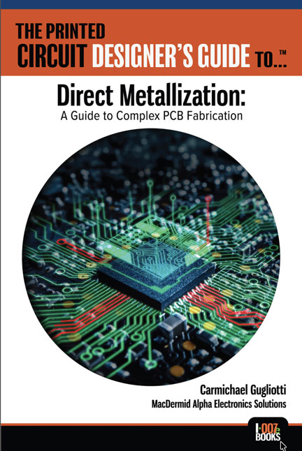
I-Connect007 Releases The Printed Circuit Designer’s Guide to… Direct Metallization: A Guide to Complex PCB Fabrication
05/12/2026 | I-Connect007As PCB complexity continues to accelerate, fabricators and OEMs are reevaluating long-standing manufacturing processes to meet the demands of AI, HDI, advanced packaging, and next-generation electronics. To address these evolving challenges, I-Connect007 is proud to announce the release of The Printed Circuit Designer’s Guide to… Direct Metallization: A Guide to Complex PCB Fabrication, authored by MacDermid Alpha Solution’s Carmichael Gugliotti.
Macnica ATD Europe Acquires Indesmatech to Deepen Engineering Presence Across Northern Europe
05/11/2026 | BUSINESS WIREMacnica ATD Europe announced the acquisition of Indesmatech, a pan-European technology and advisory company specializing in advanced semiconductor representation, design-in support and consulting, as well as point click buying services.
Dragonfly Energy Secures Additional Nevada Tech Hub Funding
05/07/2026 | Globe NewswireDragonfly Energy Holdings Corp., an industry leader in energy storage and maker of Battle Born Batteries®, announced it has been selected for a second consecutive round of funding through the Nevada Tech Hub.
Designing Without a Rulebook: When Engineering Becomes Innovation
05/05/2026 | Stephen V. Chavez, Siemens EDAWhat if the very rules that made you successful as a PCB designer are the ones now holding you back? This reminds me of walking the floor and attending sessions at both PCB West 2025 and APEX EXPO 2026, where one common theme stood out: More designs with traditional PCB “best practices” simply don’t apply. It’s not because they’re wrong, but because the problems we’re solving have fundamentally changed. In some cases, those best practices can actually limit performance. This is where PCB design moves beyond optimization and into something far more challenging: designing without a rulebook.


