


 Beyond the Board: How a Diminished Supplier Base Affects Complex PCB Manufacturing Readiness in Defense
 Defense Speak Interpreted: Hypersonics Report Back After Six Years of Silence
 American Made Advocacy: American Microelectronics Power the Future of High Technology


CIL Brings Advanced Semiconductor Solder Bumping to the UK
March 3, 2026 | CILEstimated reading time: 2 minutes
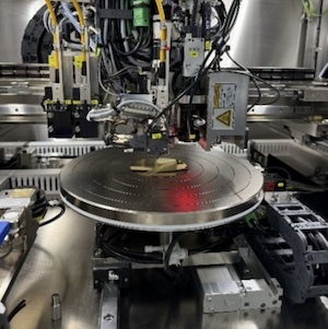
Following further investment in advanced packaging capability at its BP2 OSAT facility, CIL has brought on-line the UK’s first PacTech SB² – Jet solder ball laser reflow system. The SB² – Jet system is a three laser fully automatic balling system capable of attaching ball sizes ranging from 60um to 760um and up to 300mm wafer sizes. This will enable CIL to provide OSAT services for wafer, interposer, Flip Chip, WLCSP, CSP, PCB bumping through to BGA balling and re-balling.
As well as ball sizes from 60um to 760um, CIL will be offering advanced packaging ball attach using a selection of varying solder alloys for different market applications, these include
SAC305 - Standard RoHS alloy for most applications
SAC405 - Standard RoHS alloy for some applications
SACQ - Offers superior fatigue resistance and improved board-level reliability over SAC405 or SAC305
Tin / Lead - Defence, Mil Aero, Aerospace & Space requirement
Bismuth - Medical & Biomedical devices
CIL’s WLCSP / Flip Chip packaging services will be engaged in wide-range of industry applications, including defence, aerospace, automotive, premium motorsport, commercial, communication, industrial power, 5G and RF and many more. They are suitable for numerous assembly and packaging applications, such as:
- Flip Chip Package on Package (FC PoP)
- 3D Integrated Circuit (IC)
- 5D Interposer
- Flip Chip
- Embedded Integrated Circuit (IC)
- Fan-Out Wafer Level Packaging (FO WLP)
- Wafer Level Chip Scale Packaging (WLCSP)
- Chip Scale Packaging (CSP)
- Ball Grid Array (BGA)
- Ball Grid Array re-balling
- Printed Circuit Board (PCB) balling
The main process CIL is enabling in the UK is the manufacture of Flip Chip and WLCSP devices. These two devices are sometime confused, and they are defined as such
- Flip Chip - refers to bumps on semiconductor wafers which are in the range of 50 to 200 µm in height and are usually assembled using and underfill material between the die and the substrate
- WLCSP - refers to bumps that are in the range of 200 to 500 µm in height and are usually assembled without an underfill material
The SB² – Jet is the flagship platform of PacTech’s leading edge solder jetting technology with the high precision gantry is the most advanced system for automated high-speed sequential solder ball attach and laser reflow. With accurate, precise and reliable performance proven in mass volume production environment, the large working area of this model is highly flexible for a variety of different microelectronic substrates and applications. CIL’s comprehensive version of the SB² – Jet is complete with a vision and pattern-recognition system, an after-bump 2D inspection and an additional repair unit, wafer handling solution customizable to support customer-specific products and carriers such as conveyor, robot or reel-to-reel system, this machine is ready for in-line production integration.
Share on:


Testimonial
"Our marketing partnership with I-Connect007 is already delivering. Just a day after our press release went live, we received a direct inquiry about our updated products!"
Rachael Temple - AlltematedSuggested Items
Applications, Challenges, and the Future of Flex–Packaging Integration, Part 2
04/16/2026 | Anaya Vardya, American Standard CircuitsIn the second of this two-part series, Anaya Vardya of American Standard Circuits examines applications, challenges, manufacturing considerations, and future trends emerging from the convergence of flexible printed circuit boards and advanced semiconductor packaging. Applications driving the convergence include consumer electronics, automotive systems, medical, wearables, aerospace and more.
AI, Connectivity, and Systems-Level Thinking: New Frontiers in Advanced Packaging
04/16/2026 | I-Connect007 Editorial TeamThe upcoming issue of Advanced Electronics Packaging Digest examines key developments shaping the next phase of electronics innovation, from the reliability challenges of AI-driven packaging to emerging connectivity standards and the broader systems-level implications of artificial intelligence.
Indium Showcases Solder Alloy Reliability Research for Heterogeneous Integration at ICEP-HBS
04/15/2026 | Indium CorporationIndium Corporation Senior Global Product Manager, Semiconductor and Advanced Materials, Sze Pei Lim will present a collaborative International Electronics Manufacturing Initiative (INEMI) project comparing SnBi and SAC305 solder alloys for first-level interconnects in complex heterogeneous packages.
Camtek Receives $31 Million Multi-System Order from a Leading OSAT
04/01/2026 | CamtekCamtek Ltd., announced that it has received a multi-system order totaling $31 million from a leading OSAT mainly for CoWoS-like packaging supporting AI applications.
Global Electronics Association, MIMOS Berhad Sign MoU to Advance Malaysia’s Electronics and Semiconductor Ecosystem
03/31/2026 | Global Electronics AssociationThe Global Electronics Association and MIMOS Berhad recently signed a Memorandum of Understanding (MoU) to collaborate in strengthening Malaysia’s electronics and semiconductor ecosystem, with a focus on advanced electronic packaging (AEP), industry alignment, and global best practices.