















 It’s Only Common Sense: Why Should They Take Your Call?
 The Marketing Minute: When Everyone Is a Thought Leader, No One Is
 The Chemical Connection: More Solutions to Common PCB Etching Questions





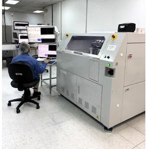
Express Manufacturing, Inc. (EMI), a global electronics manufacturing services (EMS) provider, has strengthened its test capabilities with the recent purchase of the TAKAYA APT-1600FD-SL dual-sided flying probe test system, expanding its ability to support increasingly complex and high-reliability PCB assemblies.
The addition of the APT-1600FD-SL enables EMI to perform simultaneous probing on both sides of a board, significantly improving test coverage while reducing overall test time. Designed to handle larger PCBAs, the system is well suited for emerging applications such as 5G, battery management systems (BMS), and other high-density designs that demand precise, efficient validation.
“This investment gives us more flexibility and confidence when testing today’s complex boards,” said CM Chin, Vice President of Express Manufacturing, Inc. “We’re seeing larger form factors, tighter spacing, and higher performance requirements. This system helps us keep pace while maintaining the level of quality our customers expect.”
The APT-1600FD-SL features a 10 flying Z-axis probe design, allowing access to difficult test points that traditional systems may miss. Its dual-sided configuration not only increases coverage but also shortens test cycles—helping EMI improve throughput without compromising accuracy. Integrated laser profiling further enhances precision by compensating for board warpage prior to testing, ensuring consistent contact and reliable results.
For EMI customers, the benefits are immediate:
- Higher test coverage for complex and densely populated PCB assemblies
- Faster turnaround times driven by reduced test cycles and improved throughput
- Improved product quality through more accurate and repeatable testing
- Support for larger boards and next-generation applications
The system also incorporates advanced measurement capabilities and high-resolution vision inspection, enabling EMI to detect defects such as missing components, incorrect placement, and orientation issues earlier in the process.
“As designs continue to evolve, test has to evolve with them,” added Chin “This is about giving our customers the assurance that their products are fully validated before they leave our floor.”
The investment reflects EMI’s ongoing focus on building a robust, scalable manufacturing environment that supports both current production needs and future technologies.


