


 Dan’s Biz Bookshelf: ‘The Soul of a New Machine’
 The Chemical Connection: Back to Basic Cupric Chloride Etching
 The Marketing Minute: The Tyranny of the Dashboard


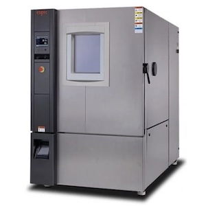
JAVAD EMS (JEMS), a leading global EMS company that provides low to medium volume, high-mix applications, has ordered a new ESPEC EGNZ28-15NW temperature cycling chamber to expand its environmental testing capabilities as demand continues to grow in the military and aerospace sectors.
The chamber supports a temperature range from -70°C to 180°C and faster ramp rates of up to 15°C per minute under load, giving JEMS the ability to meet newer program requirements and shorten overall test cycles.
“We’re seeing more programs that call for tighter testing requirements and increased throughput,” said Gary Walker, President of JAVAD EMS. “This equipment helps us keep pace with those requirements and gives us more flexibility in how we schedule and run tests.”
The ESPEC Global-N chamber offers a temperature range from -70°C to 180°C and a large 28 cubic foot workspace, allowing JEMS to handle complex assemblies and larger builds. Features such as dual-zone airflow, precise temperature control, and a robust refrigeration system support consistent, repeatable test results.
JAVAD EMS focuses on low- to medium-volume, high-mix manufacturing for applications where reliability matters, including aerospace, subsea, satellite, and secure communications. The company supports complex assemblies with capabilities such as fine-pitch and high-density PCBA, along with advanced inspection including 3D solder paste inspection, automated optical inspection, and 3D X-ray.
Adding this chamber strengthens JEMS’ ability to validate products under extreme conditions before they move into the field, while maintaining full traceability throughout the build and test process.
JEMS expects to continue expanding its environmental testing capacity, with plans to add another high-capacity temperature chamber later this year.


