


 Standard of Excellence: The Future of Fabrication—From Art to Automation
 Knocking Down the Bone Pile: The Business Case for Component Reclamation
 Global Sourcing Spotlight: The Hidden Power of the Rep Network


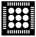
Requirements for void-free solder joints are continuously increasing in the field of electronics manufacturing (i.e., the reduction or elimination of cavities in the connection technology used between component connectors and connector pads). New challenges evolve on a daily basis due to the relentless introduction of new variants of so-called bottom-terminated components (BTCs), some of which are shown in Figure 1. Connector geometries alone are not decisive—numerous pitfalls are of greater significance. Incentives and several fundamentals will be elucidated in the following article.
The formation of solder joints is PCB manufacturing, and thus their quality, is influenced by an unmanageably large number of parameters, which are becoming increasingly difficult to master and control. A voids workgroup prepared the overview of factors shown in Figure 2, which provides an initial insight into the complexity of the problem. However, it only includes two factors that can be taken advantage of shortly before production of the affected PCBs in order to reduce or eliminate the formation of voids. These are the stencil and the layout of the aperture on the one hand, and the use of vacuum technology during the soldering process itself on the other hand. Vacuum soldering can even be used during the production processes as a sort of fire brigade when a short-term increase in the number of voids occurs. Thus, nothing stands in the way of using standard processes and standard profiles for series production; it’s possible to react flexibly to any fluctuation in the quality of purchased components, PCB surfaces and solder paste batches.
In addition to series production, PCBs can also be repaired in modern vacuum soldering systems like the CondensoX, in the event that excessively large voids have occurred during the initial soldering process in a conventional soldering system, which would otherwise have to be scrapped because they do not fulfill the criteria of the applicable IEC standards or IPC directives.
Vacuum is defined as follows in DIN 28400 (in agreement with ISO 3529-1):
“Vacuum is the state of a gas when the pressure of the gas, and thus the particle-number density, is lower within than it is outside of its container, or when the pressure of the gas is less than 300 mbar (i.e., lower than the smallest atmospheric pressure which occurs on the surface of the Earth.”)Page 1 of 2


