-
- News
- Books
Featured Books
- I-Connect007 Magazine
Latest Issues
Current Issue
Beyond the Rulebook
What happens when the rule book is no longer useful, or worse, was never written in the first place? In today’s fast-moving electronics landscape, we’re increasingly asked to design and build what has no precedent, no proven path, and no tidy checklist to follow. This is where “Design for Invention” begins.
March Madness
From the growing role of AI in design tools to the challenge of managing cumulative tolerances, these articles in this issue examine the technical details, design choices, and manufacturing considerations that determine whether a board works as intended.
Looking Forward to APEX EXPO 2026
I-Connect007 Magazine previews APEX EXPO 2026, covering everything from the show floor to the technical conference. For PCB designers, we move past the dreaded auto-router and spotlight AI design tools that actually matter.
- Articles
- Columns
- Links
- Media kit
||| MENU - I-Connect007 Magazine
Optimization of Acid Copper Electrodeposition Processes for High-Throwing Power DC Plating
June 2, 2015 | Michael Carano, RBP Chemical TechnologyEstimated reading time: 1 minute
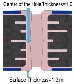
Perhaps one of the three most fundamental aspects of printed circuit fabrication is the metallization and electroplating of throughhole vias and blind via interconnections. Ideally, one should also include fine-line imaging of increasingly smaller feature sizes and via formation, whether by mechanical or laser methods.
Indeed, the foundation of technology roadmaps should, at the very least, encompass a discussion of line widths and spaces, PTH and blind via aspect ratios, and a metric that defines acceptability of plating uniformity and throwing power. These same parameters have been used for nearly four decades to quickly quantify the capability of a fabricator to profitably produce traditional boards. The ability to image conductor lines, and perhaps even more important, the insulating airspace between them, is considered a key characteristic. With surface mount components, a dramatic decrease in plated via hole diameter requirements occurred, and as a result, via holes have become simple vertical interconnections. Now, under competition from laser drilling, both drill bit and machine technology have driven mechanical holes capability much smaller.
In the most recent release of the IPC Technology Roadmap, PTH and blind via diameters and aspect ratios have been defined as to the technology sector where the boards are used. In order to provide a list of key attributes (layer counts, board thickness, number and diameters of vias, etc.) for the PCB, emulators are employed. Emulators (synthetic) are representations of a category of product, combining the attributes common to the type to avoid concerns about disclosure of specific company-proprietary designs. Technologists from around the world were asked to provide their respective view of the PCB technology required for the emulator. This exercise is critical in developing and understanding roadmaps.
Editor's Note: This article originally appeared in the May 2015 issue of The PCB Magazine.
Testimonial
"We’re proud to call I-Connect007 a trusted partner. Their innovative approach and industry insight made our podcast collaboration a success by connecting us with the right audience and delivering real results."
Julia McCaffrey - NCAB GroupSuggested Items
The Missing Connection: Wire Harness Quoting Joins the Digital Age
05/01/2026 | Joanne Harris, Tech-2marketingWalk the floor of a modern wire harness manufacturing facility, and the investment in technology is hard to miss. Automated wire cutting and stripping machines process thousands of cuts an hour with sub-millimeter precision. Computerized crimping presses deliver consistent, validated terminations that a hand tool never could. Laser wire markers, automated test benches, and vision-guided assembly stations represent hundreds of thousands of dollars of capital investment, all in service of building a better harness faster and more reliably than the competition.
Everspin Executes $40M Agreement for Mil-Aero MRAM Applications
05/01/2026 | Everspin Technologies, Inc.Everspin Technologies, Inc., the world’s leading developer and manufacturer of Magnetoresistive Random Access Memory (MRAM) persistent memory solutions, announced an agreement with a U.S. prime contractor to provide state-of-the-art Toggle MRAM process technology capabilities and engineering services for United States Defense Industrial Base customers.
Everspin Executes $40M Agreement for Mil-Aero MRAM Applications
04/30/2026 | Everspin Technologies, Inc.Everspin Technologies, Inc., the world’s leading developer and manufacturer of Magnetoresistive Random Access Memory (MRAM) persistent memory solutions, announced an agreement with a U.S. prime contractor to provide state-of-the-art Toggle MRAM process technology capabilities and engineering services for United States Defense Industrial Base customers.
Swinburne University, Siemens Launch Australia’s First Quantum Timing Study for Smarter Power Grids
04/30/2026 | SiemensSwinburne University of Technology and Siemens are undertaking first-of-its-kind research in Australia, into how quantum-enhanced timing can help future-proof the energy grid and increase grid stability.
A Designer's Focus on High Density
04/30/2026 | Marcy LaRont, I-Connect007 MagazineVern Solberg is a distinguished member of the Global Electronics Association Raymond E. Pritchard Hall of Fame and has served as chair or vice chair of many committees, developing technical standards and implementation guidelines, including the IPC-7090 series, which focuses on design for manufacturing and reliability for electronic assemblies. He’s a long-time contributor to Design007 Magazine, and he conducted a half-day tutorial at APEX EXPO 2026, where he addressed 2D, 2.5D, and 3D packaging and ultra-high density hybrid bond interconnect. I caught up with Vern at the show and asked about his pivot from addressing more standard design challenges to his focus on high-density circuits.