


 Dan’s Biz Bookshelf: ‘In Defense of a Liberal Education’
 American Made Advocacy: A Growing Presence in Washington in Turbulent Times


Electroplating Through-Holes with Different Geometry: A Novel and High-Productivity Process
June 4, 2015 | Cirexx InternationalEstimated reading time: 1 minute
Microfill through-hole fill (THF) electrolytic copper is a new process designed to offer outstanding through-hole fill, particularly for substrates intended for use as core layers in build–up applications, producing planar, solid copper plugs in high-volume production plating equipment. This technology is intended to replace resin or paste plugging, and offers many advantages, including improved reliability, higher electrical and thermal conductivity, increased productivity and reduced process costs.
This paper describes a novel copper through-hole fill electroplating process designed for use with insoluble anodes and direct current (DC) rectification. The copper through-hole fill chemistry is formulated to operate over a broad range of operating conditions, and offers end-users outstanding production flexibility in either panel or pattern plate operating mode.
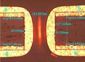
The paper addresses electrolytic copper through-hole filling performance for a variety of substrate thicknesses and hole diameters. The impact of the hole formation method and hole quality on filling ratio and void formation will be discussed. In this work, production scale tests were performed on 100 μm and 200μm thick substrates. The impacts of varying current density and solution flow on hole filling were examined. With optimized deposition conditions, including on-line additive analysis, void-free, highly planar through-hole filling and excellent bottom-up blind microvia filling with low surface copper deposition thickness were demonstrated.
Portability of consumer electronics has become the primary driver for the ever-increasing circuit density of today’s printed circuit designs. Based on the small dimensions of these devices, through-hole and blind via diameters are typically in the 75–150 µm range. Performance improvement and process cost reduction make through-hole filling technology with copper an excellent approach, rather than the conventional plated through-hole.
Prior to the development of electrolytic copper through-hole filling, substrates for such applications were electroplated with a conventional through-hole process, then plugged with an epoxy material. Following these steps, additional planarization, re-metallization and electrolytic copper capping processes were required before the build-up process steps could begin.
Use of electrolytic copper through-hole filling eliminates several of these manufacturing steps and offers a number of additional advantages over the conventional build-up process by enhancing the thermal and electrical conductivity of the interconnections, and by reducing overall costs.
Editor's Note: This article originally appeared in the May 2015 issue of The PCB Magazine.
Share on:


Testimonial
"We’re proud to call I-Connect007 a trusted partner. Their innovative approach and industry insight made our podcast collaboration a success by connecting us with the right audience and delivering real results."
Julia McCaffrey - NCAB GroupSuggested Items
Statement from the Global Electronics Association on the July 2025 Tariff on Copper Foil and Electronics-Grade Copper Inputs
07/31/2025 | Global Electronics AssociationWe are disappointed by today’s decision to impose a 50% tariff on imported copper foil and other essential materials critical to electronics manufacturing in the United States.
Considering the Future of Impending Copper Tariffs
07/30/2025 | I-Connect007 Editorial TeamThe Global Electronics Association is alerting industry members that a potential 50% tariff on copper could hit U.S. electronics manufacturers where it hurts.
Connect the Dots: Sequential Lamination in HDI PCB Manufacturing
07/31/2025 | Matt Stevenson -- Column: Connect the DotsAs HDI technology becomes mainstream in high-speed and miniaturized electronics, understanding the PCB manufacturing process can help PCB design engineers create successful, cost-effective designs using advanced technologies. Designs that incorporate blind and buried vias, boards with space constraints, sensitive signal integrity requirements, or internal heat dissipation concerns are often candidates for HDI technology and usually require sequential lamination to satisfy the requirements.
OKI Launches Rigid-Flex PCBs with Embedded Copper Coins Featuring Improved Heat Dissipation for Space Equipment Applications
07/29/2025 | BUSINESS WIREOKI Circuit Technology, the OKI Group’s printed circuit board (PCB) business company, has developed rigid-flex PCBs with embedded copper coins that offer improved heat dissipation for use in rockets and satellite-mounted equipment operating in vacuum environments.
Designers Notebook: Basic PCB Planning Criteria—Establishing Design Constraints
07/22/2025 | Vern Solberg -- Column: Designer's NotebookPrinted circuit board development flows more smoothly when all critical issues are predefined and understood from the start. As a basic planning strategy, the designer must first consider the product performance criteria, then determine the specific industry standards or specifications that the product must meet. Planning also includes a review of all significant issues that may affect the product’s manufacture, performance, reliability, overall quality, and safety.