


 The Marketing Minute: Cracking the Code of Technical Marketing
 Trouble in Your Tank: Implementing Direct Metallization in Advanced Substrate Packaging


Novel Microscope for Nanosystems
June 25, 2015 | Max-Planck-Gesellschaft, MünchenEstimated reading time: 3 minutes
Nanomaterials play an essential role in many areas of daily life. There is thus a large interest to gain detailed knowledge about their optical and electronic properties. Conventional microscopes get beyond their limits when particle size falls to the range of a few ten nanometers where a single particle provides only a vanishingly small signal. As a consequence, many investigations are limited to large ensembles of particles. Now, a team of scientists of the Laser Spectroscopy Division of Prof. Theodor W. Hänsch (Director at the Max Planck Institute of Quantum Optics and Chair for Experimental Physics at the Ludwig-Maximilians-Universität Munich) has developed a technique, where an optical microcavity is used to enhance the signals by more than 1000-fold and at the same time achieves an optical resolution close to the fundamental diffraction limit. The possibility to study the optical properties of individual nanoparticles or macromolecules promises intriguing potential for many areas of biology, chemistry, and nanoscience (Nature Communications, DOI: 10.1038/ncomms8249, 24 June 2015).
Spectroscopic measurements on large ensembles of nanoparticles suffer from the fact that individual differences in size, shape, and molecular composition are washed out and only average quantities can be extracted. There is thus a large interest to develop single-particle-sensitive techniques. “Our approach is to trap the probe light used for imaging inside of an optical resonator, where it circulates tens of thousands of times. This enhances the interaction between the light and the sample, and the signal becomes easily measurable”, explains Dr. David Hunger, one of the scientists working on the experiment. “For an ordinary microscope, the signal would be only a millionth of the input power, which is hardly measurable. Because of the resonator, the signal gets enhanced by a factor of 50000.”
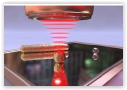
In the microscope, built by Dr. David Hunger and his team, one side of the resonator is made of a plane mirror that serves at the same time as a carrier for the nanoparticles under investigation. The counterpart is a strongly curved mirror on the end facet of an optical fibre. Laser light is coupled into the resonator through this fibre. The plane mirror is moved point by point with respect to the fibre in order to bring the particle step by step into its focus. At the same time, the distance between both mirrors is adjusted such that the condition for the appearance of resonance modes is fulfilled. This requires an accuracy in the range of picometers.
For their first measurements, the scientists used gold spheres with a diameter of 40 nanometers. “The gold particles serve as our reference system, as we can calculate their properties precisely and therefore check the validity of our measurements” says David Hunger. “Since we know the optical properties of our measurement apparatus very accurately, we can determine the optical properties of the particles from the transmission signal quantitatively and compare it to the calculation”. In contrast to other methods relying on direct signal enhancement, the light field is limited to a very small area, such that by using only the fundamental mode, a spatial resolution of 2 micron is achieved. By combining higher order modes, the scientists could even increase the resolution to around 800 nanometers.
The method becomes even more powerful when both absorptive and dispersive properties of a single particle were determined at the same time. This is interesting especially if the particles are not spherical but e.g. elongated. Then, the corresponding quantities depend on the orientation of the polarization of light with respect to the symmetry axes of the particle. “In our experiment we use gold nanorods (34x25x25 nm³) and we observe how the resonance frequency shifts depending on the orientation of the polarization. If the polarization is oriented parallel to the axes of the rod, the shift of the resonance is larger than if the polarization is oriented orthogonally, resulting in two different resonance frequencies for both orthogonal polarizations” explains Matthias Mader, PhD student at the experiment. “This birefringence can be measured very precisely and is a very sensitive indicator for the shape and orientation of the particle.”
“As an application of our method, we could think of e.g. investigating the temporal dynamics of macro molecules, such as the folding dynamics of proteins” says David Hunger. “Overall we see a large potential for our method: from the characterization of nanomaterials and biological nanosystems to spectroscopy of quantum emitters.” [OM/DH]
Share on:


Testimonial
"The I-Connect007 team is outstanding—kind, responsive, and a true marketing partner. Their design team created fresh, eye-catching ads, and their editorial support polished our content to let our brand shine. Thank you all! "
Sweeney Ng - CEE PCBSuggested Items
MEMS & Imaging Sensors Summit to Spotlight Sensing Revolution for Europe’s Leadership
09/11/2025 | SEMIIndustry experts will gather November 19-20 at the SEMI MEMS & Imaging Sensors Summit 2025 to explore the latest breakthroughs in AI-driven MEMS and imaging optimization, AR/VR technologies, and advanced sensor solutions for critical defence applications.
Direct Imaging System Market Size to Hit $4.30B by 2032, Driven by Increasing Demand for High-Precision PCB Manufacturing
09/11/2025 | Globe NewswireAccording to the SNS Insider, “The Direct Imaging System Market size was valued at $2.21 Billion in 2024 and is projected to reach $4.30 Billion by 2032, growing at a CAGR of 8.68% during 2025-2032.”
I-Connect007’s Editor’s Choice: Five Must-Reads for the Week
07/04/2025 | Marcy LaRont, I-Connect007For our industry, we have seen several bullish market announcements over the past few weeks, including one this week by IDC on the massive growth in the global server market. We’re also closely watching global trade and nearshoring. One good example of successful nearshoring is Rehm Thermal Systems, which celebrates its 10th anniversary in Mexico and the official opening of its new building in Guadalajara.
Driving Innovation: Direct Imaging vs. Conventional Exposure
07/01/2025 | Simon Khesin -- Column: Driving InnovationMy first camera used Kodak film. I even experimented with developing photos in the bathroom, though I usually dropped the film off at a Kodak center and received the prints two weeks later, only to discover that some images were out of focus or poorly framed. Today, every smartphone contains a high-quality camera capable of producing stunning images instantly.
United Electronics Corporation Advances Manufacturing Capabilities with Schmoll MDI-ST Imaging Equipment
06/24/2025 | United Electronics CorporationUnited Electronics Corporation has successfully installed the advanced Schmoll MDI-ST (XL) imaging equipment at their advanced printed circuit board facility. This significant technology investment represents a continued commitment to delivering superior products and maintaining their position as an industry leader in precision PCB manufacturing.