


 Nolan’s Notes: Everyone Has Their Eye on India
 Standard of Excellence: The Human Touch in an Automated World
 The Government Circuit: Navigating New Trade Headwinds and New Partnerships


Reliability Study of Bottom Terminated Components (Part 1)
July 6, 2015 | J. Nguyen, H. Marin, D. Geiger, A. Mohammed, and M. Kurwa, Flextronics InternationalEstimated reading time: 6 minutes
Bottom terminated components (BTC) are leadless components where terminations are protectively plated on the underside of the package. They are all slightly different and have different names, such as QFN (quad flat no lead), DFN (dual flat no lead), LGA (land grid array) and MLF (micro lead-frame. BTC assembly has increased rapidly in recent years. This type of package is attractive due to its low cost and good performance like improved signal speeds and enhanced thermal performance.
However, bottom terminated components do not have any leads to absorb the stress and strain on the solder joints. It relies on the correct amount of solder deposited during the assembly process for having a good solder joint quality and reliable reliability. Voiding is typically seen on the BTC solder joint, especially on the thermal pad of the component. Voiding creates a major concern on BTC component’s solder joint reliability. There is no current industry standard on the voiding criteria for bottom terminated component. The impact of voiding on solder joint reliability and the impact of voiding on the heat transfer characteristics at BTC component are not well understood. This paper will present some data to address these concerns. We will present our study on the thermal cycling reliability of bottom terminated components, including non-symmetrical LGA and QFN components. Two different solder process conditions and different voiding levels were included in the study, and the results will be discussed. The paper also covers our thermal modeling study of the heat transfer characteristic of BTC component.
Introduction
BTC is known as bottom terminated component or bottom termination component. It is a leadless component for which the termination is protectively plated and is on the underside of the package. Common BTC components include QFN (quad flat no lead), LGA (land grid array), MLF (micro lead-frame), DFN (dual flat no lead), etc. BTC components are available in different sizes, lead counts, and designs. Most parts are unique from supplier to supplier with various pad designs.
Most BTC components typically have a large ground or power termination along with smaller signal terminations. Voiding is commonly seen at the solder joint of BTC components, especially at the thermal pads. In many cases, large voids and many voids which can exceed 25% of the area can be seen at the thermal pads of BTC components. Voiding causes many concerns for the solder joint reliability of BTC components. The following questions are typical when dealing with BTC: Will the excessive voiding decrease the solder joint reliability? Will the voiding impact the heat transfer and thermal behavior of the BTC component? In this paper, we will present our study on the thermal cycling reliability of BTC components. Voiding and reliability data will be compared. We will discuss the heat transfer characteristic of BTC component using our thermal modeling study.
Experimental Details
Test Vehicle
The company's Bottom Terminated Component Test Vehicle, Rev 1.0 was used in the study (Figure 1a). It is a double sided board with the dimension of 8” x 11” x 0.093” [203mmx279mmx2.4mm]. Thirteen different BTC component types from various suppliers were designed into the test vehicle (Figure 1b). It also had other components such as BGA, SMT connector, and chip components among others.
Figure 1: Company Bottom Terminated Component Test Vehicle a) Topside b) Various BTC Pad Design.
Components
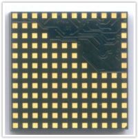
Table 1 summarizes the component details tested in the reliability study. Both QFN and LGA component types were included in the reliability testing. We also included a BGA and FQFP component for data comparison. For the QFN component type, we had both symmetrical QFN (Figure 2) and non-symmetrical QFN components in the study (Figure 3). For the LGA component type, some LGA components had the same pad sizes for both signal and ground pins (Figure 4). Some other LGA components had various pad sizes for signal and ground pins (Figure 5).
Figure 2: Symmetrical QFN Component Images. a) QFN 88 b) Dual Row QFN132
Figure 3: Non-symmetrical QFN Component Images.
Figure 4: LGA Images_ Identical Pad Size for Signal and Ground Pins.
Sample Preparation
Previous studies [1-2] showed that more solder generally resulted in less voiding. To study the impact of voiding on reliability, we built boards using two different process conditions to simulate different voiding levels in the solder joint. In one process condition, boards were built using a regular stencil which resulted in more voids in the solder joint. In the other process condition, pre-tinned components were used. This condition typically had less voiding in the solder joint.
Page 1 of 3
Share on:


Testimonial
"Our marketing partnership with I-Connect007 is already delivering. Just a day after our press release went live, we received a direct inquiry about our updated products!"
Rachael Temple - AlltematedSuggested Items
Absolute EMS: The Science of the Perfect Solder Joint
09/05/2025 | Absolute EMS, Inc.Absolute EMS, Inc., a six-time award-winning provider of fast turnaround, turnkey contract electronic manufacturing services (EMS), is drawing attention to the critical role of 3D Solder Paste Inspection (SPI) in ensuring the reliability of both FLEX and rigid printed circuit board assemblies (PCBAs).
Indium Corporation to Highlight High-Reliability Solder Solutions at SMTA Guadalajara Expo
09/04/2025 | Indium CorporationIndium Corporation, a leading materials refiner, smelter, manufacturer, and supplier to the global electronics, semiconductor, thin-film, and thermal management markets, will feature a range of innovative, high-reliability solder products for printed circuit board assembly (PCBA) at the SMTA Guadalajara Expo and Tech Forum, to be held September 17-18 in Guadalajara, Mexico.
Dr. Jennie Hwang to Present on ‘Solder Joint Reliability’ at SMTA International 2025
09/03/2025 | Dr. Jennie HwangDr. Jennie Hwang to address “Solder Joint Reliability” at the 2025 SMTA International Conference on Monday, October 20. Leveraging her decades of extensive real-world experiences and deep knowledge,
Indium to Highlight Energy-Efficient, High-Reliability Solder Solutions for EV and Electronics at Productronica India
09/03/2025 | Indium CorporationIndium Corporation, a leading materials refiner, smelter, manufacturer, and supplier to the global electronics, semiconductor, electric vehicle (EV), thin-film, and thermal management markets, will feature a range of sustainable, high-reliability solder products at Productronica India, to be held September 17-19 in Bengaluru, India.
Altus Supports Datalink Electronics with Advanced Selective Soldering Solution to Boost Manufacturing Efficiency
09/02/2025 | Altus GroupDatalink Electronics has partnered with Altus Group to integrate a cutting-edge automated soldering solution, enhancing its production capabilities and reinforcing its strategic focus on quality, automation, and scalability.