


 Nolan’s Notes: Everyone Has Their Eye on India
 Standard of Excellence: The Human Touch in an Automated World
 The Government Circuit: Navigating New Trade Headwinds and New Partnerships


Reliability Study of Bottom Terminated Components (Part 1)
July 6, 2015 | J. Nguyen, H. Marin, D. Geiger, A. Mohammed, and M. Kurwa, Flextronics InternationalEstimated reading time: 6 minutes
Results and Discussions
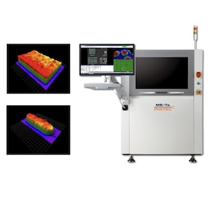
X-Ray Inspection
Pre-tinned BTC components generally had less voiding than non-pre-tinned BTC components. However, voiding varied depending on the component type. Most of the components had an average void % of less than 25% except the dual row QFN132 component and FQFP176 component (Figure 7a). Maximum void percentage was seen up to 30%, 40%, 50%, depending on the component type, its pad size and process condition (Figure 7b).
Figure 7: Solder Joint Voiding Comparison for Sample Built with Pre-tinned BTC vs. Regular BTC. a) Average Void% b) Maximum void %.
Pre-tinned components did not eliminate voids. However, the size of the voids in the pre-tinned samples was typically smaller than the voids of solder joints using non pre-tinned component (Figure 8). The shape of the voids for pre-tinned sample was more defined and circular as compared to the non-pre-tinned solder joint sample (Figure 9).
Figure 8: X-Ray Images of QFN 3550 Solder Joint Assembled with Non-Pre-tinned Component vs. Pre-tinned Component.
Figure 9: X-Ray Images of QFN132 Solder Joint Assembled with Non-Pre-Tinned Component vs. Pre-Tinned Component.
Solder Joint Microstructure – Time Zero Analysis
Cross sections of the BTC solder joints were performed to evaluate the solder joint microstructure and inter-metallic formation at time zero (prior to thermal cycle testing). Non-pre-tinned components had a standoff height of about 2mil to 3.5mil, depending on the component type. The pre-tinned component standoff height was between 4-7mil. It was approximately twice of the non-pre-tinned component standoff [Table 2]. The BGA196 component had a standoff height of around 11mil.
Table 2: Solder Joint Standoff Height of BTC Assembled Using Regular Process and Pre-tinned Components
Good solder joint wetting and normal IMC layers were observed for all the components. No cracked solder joints were found at time-zero for all the samples (Figure 10, Figure 11 and Figure 12).
Figure 10: Cross Section Images of a QFN component at t=0_ Non-Pre-tinned Component.
Figure 11: Cross Section Images of a QFN Component after Reflow_ Using Pre-tinned Components.
Figure 12: Cross Section Images of BGA Component after Reflow.
In Part 2 of this two-part article series, failure analysis after thermal cycle tests will be discussed, as well as the impact of solder voids in the thermal pad of the BTC.
Editor's Note: This paper has been published in the technical proceedings of IPC APEX EXPO.
Page 3 of 3Share on:


Testimonial
"Our marketing partnership with I-Connect007 is already delivering. Just a day after our press release went live, we received a direct inquiry about our updated products!"
Rachael Temple - AlltematedSuggested Items
Absolute EMS: The Science of the Perfect Solder Joint
09/05/2025 | Absolute EMS, Inc.Absolute EMS, Inc., a six-time award-winning provider of fast turnaround, turnkey contract electronic manufacturing services (EMS), is drawing attention to the critical role of 3D Solder Paste Inspection (SPI) in ensuring the reliability of both FLEX and rigid printed circuit board assemblies (PCBAs).
Indium Corporation to Highlight High-Reliability Solder Solutions at SMTA Guadalajara Expo
09/04/2025 | Indium CorporationIndium Corporation, a leading materials refiner, smelter, manufacturer, and supplier to the global electronics, semiconductor, thin-film, and thermal management markets, will feature a range of innovative, high-reliability solder products for printed circuit board assembly (PCBA) at the SMTA Guadalajara Expo and Tech Forum, to be held September 17-18 in Guadalajara, Mexico.
Dr. Jennie Hwang to Present on ‘Solder Joint Reliability’ at SMTA International 2025
09/03/2025 | Dr. Jennie HwangDr. Jennie Hwang to address “Solder Joint Reliability” at the 2025 SMTA International Conference on Monday, October 20. Leveraging her decades of extensive real-world experiences and deep knowledge,
Indium to Highlight Energy-Efficient, High-Reliability Solder Solutions for EV and Electronics at Productronica India
09/03/2025 | Indium CorporationIndium Corporation, a leading materials refiner, smelter, manufacturer, and supplier to the global electronics, semiconductor, electric vehicle (EV), thin-film, and thermal management markets, will feature a range of sustainable, high-reliability solder products at Productronica India, to be held September 17-19 in Bengaluru, India.
Altus Supports Datalink Electronics with Advanced Selective Soldering Solution to Boost Manufacturing Efficiency
09/02/2025 | Altus GroupDatalink Electronics has partnered with Altus Group to integrate a cutting-edge automated soldering solution, enhancing its production capabilities and reinforcing its strategic focus on quality, automation, and scalability.