


 It’s Only Common Sense: Hire for Hunger, Train for Skill
 Dan’s Biz Bookshelf: ‘The 'NVIDIA Way: Jensen Huang and the Making of a Tech Giant’


Research Improves Efficiency from Larger Perovskite Solar Cells
October 6, 2015 | Brown UniversityEstimated reading time: 2 minutes
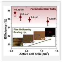
Using a newly developed fabrication method, a research team has attained better than a 15-percent energy conversion efficiency from perovskite solar cells larger than one square centimeter area. The researchers, from Brown University and the National Renewable Energy Lab (NREL), have reported their findings in the journal Advanced Materials.
Perovskites, materials with a particular crystalline structure, have caused quite a buzz in the solar energy world. Perovskite solar cells are relatively cheap to make, and the efficiency with which they can convert sunlight into electricity has been increasing rapidly in recent years. Researchers have reported efficiency in perovskite cells of higher than 20 percent, which rivals traditional silicon cells. Those high efficiency ratings, however, have been achieved using cells only a tenth of a square centimeter -- fine for lab testing, but too small to be used in a solar panel.
"The use of tiny cells for efficiency testing has prompted some to question comparison of perovskite solar cells with other established photovoltaic technologies," said Nitin Padture, professor of engineering at Brown, director of Brown's Institute for Molecular and Nanoscale Innovation, and one of the senior authors of the new research. "But here we have shown that it is feasible to obtain 15-percent efficiency on cells larger than a square centimeter through improved processing. This is real progress."
Maintaining high efficiency on larger perovskite cells has proved to be a challenge, Padture says. "The problem with perovskite has been that when you try to make larger films using traditional methods, you get defects in the film that decrease efficiency."
The fabrication process that the Brown and NREL researchers reported in this latest paper builds on a previously reported method developed by Yuanyuan Zhou, a graduate student in Padture's lab. Perovskite precursors are dissolved in a solvent and coated onto a substrate. Then the substrate is bathed in a second solvent (called anti-solvent) that selectively grabs the precursor-solvent and whisks it away. What's left is an ultra-smooth film of perovskite crystals.
In this new study Zhou and Mengjin Yang, a postdoctoral researcher at NREL, developed a trick to grow the perovskite crystals to a larger size. The trick is to add excess organic precursor that initially "glues" the small perovskite crystals and helps them merge into larger ones during a heat-treatment, which then bakes away the excess precursor.
"The full coverage and uniformity over a large area come from the solvent method," Padture said. "Once we have that coverage, then we increase the size of the crystals. That gives us a film with fewer defects and higher efficiency." The 15-percent efficiency reached in this latest work is a good start, Padture said, but there's still room to improve. Ultimately, he would like to reach 20 to 25 percent in large-area cells, and he thinks that mark could be within reach using this method or a similar one.
Padture and colleagues at the University of Nebraska-Lincoln were recently awarded a $4-million grant by the National Science Foundation to expand their perovskite research.
Share on:


Testimonial
"Your magazines are a great platform for people to exchange knowledge. Thank you for the work that you do."
Simon Khesin - Schmoll MaschinenSuggested Items
Flexible Thinking: Designing Flex Circuits for Dynamic Reliability
04/09/2026 | Joe Fjelstad -- Column: Flexible ThinkingFlex circuits flex. No surprises there. However, they are also very commonly designed into products because they are thin and offer consistent thickness and dielectric properties, attributes highly prized by present-day product designers of personal electronics. This would include smartphones and, increasingly, wearable electronics for medical monitoring and even fashion.
My Top 7 Takeaways from APEX EXPO 2026
04/03/2026 | Chris Mitchell, VP of Global Government Relations, Global Electronics AssociationI’m back from APEX EXPO 2026 in Anaheim, California, and it was another great year. Even amid significant global volatility, the industry is growing, innovating, and building partnerships. As I reflect on the experience, I want to share my top 7 takeaways and explain why each matters. First is this year’s Advanced Electronics Packaging Conference (AEPC) , which delivered outstanding, peer-reviewed content and strong participation, reflecting how central advanced electronics packaging has become across the industry.
APEX EXPO Opens Today With Ribbon Cutting and Sold-Out Show Floor
03/17/2026 | Michelle Te, I-Connect007APEX EXPO officially opens today with a ribbon-cutting ceremony welcoming attendees onto the sold-out show floor in Anaheim, California. Standards committee meetings and professional development courses have been underway since the weekend, but Tuesday marks the official opening of the exhibition as more than 400 exhibitors prepare to showcase their latest equipment, materials, and technologies across 140,000 square feet of exhibit space.
Finding Your Marketing Niche in a Crowded PCB Industry
03/10/2026 | Richard Nichols, GreenSource EngineeringI recently made a flippant comment on LinkedIn, “All marketing and no trousers,” hinting that marketing campaigns often do not have a tangible product to market and the campaign is marketing a concept or a gut feeling. For PCB and IC substrate manufacturers, this poses a great risk for unsuccessful campaigns and the opportunity to innovate in an increasingly competitive and global landscape.
Beyond the Board: How Advanced PCB Design Is Reshaping Mil/Aero Electronics
03/10/2026 | Jesse Vaughan -- Column: Beyond the BoardAs mil/aero electronics evolve toward higher data rates, greater processing density, and tighter mechanical envelopes, integration is no longer occurring primarily at the box level, but rather deep within the electronic architecture itself, often beginning at the printed circuit board.