


 Dan’s Biz Bookshelf: Four Important Books You Need to Read (Not Just Say You Have)
 The Marketing Minute: Cracking the Code of Technical Marketing


Room Temperature Magnetic Skyrmions, A New Type of Digital Memory?
October 9, 2015 | NISTEstimated reading time: 2 minutes
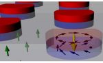
An exotic, swirling object with the sci-fi name of a "magnetic skyrmion" could be the future of nanoelectronics and memory storage. Physicists at UC Davis and the National Institute of Standards and Technology (NIST) have now succeeded in making magnetic skyrmions, formerly found at temperatures close to absolute zero, at room temperature.
"This is a potentially new way to store information, and the energy costs are expected to be extremely low," said Kai Liu, professor of physics at UC Davis and corresponding author of a paper on the work, published in the journal Nature Communications Oct. 8.
Skyrmions were originally described over 50 years ago as a type of hypothetical particle in nuclear physics. Actual magnetic skyrmions were discovered only in 2009, as chiral patterns of magnetic moments -- think of a moment as a tiny compass needle -- in materials close to absolute zero temperature, in the presence of a strong magnetic field.
Magnetic skyrmions fall into two types, Liu said: "Bloch skyrmions," with a hurricane-like spiral pattern of magnetic moments around a perpendicular center, surrounded by magnetic moments oriented in the opposite direction to the center; and "hedgehogs," where the magnetic moments orient like spikes on a hedgehog or sea urchin.
The interesting thing about magnetic skyrmions, Liu said, is that they are "topologically protected:" they can be continuously deformed, in the same way that a coffee mug shape can be deformed into a bagel shape, but they do not readily go back into a state where all the magnetic moments are aligned. That means they can potentially store information at an energy cost much lower than current technology, Liu said.
Together with graduate student Dustin Gilbert, now a postdoctoral fellow at NIST, Liu and colleagues designed a nanosynthesis approach to achieve artificial "Bloch" magnetic skyrmions at room temperature. They created a pattern of magnetic nanodots, each about half a micron across, on a multilayered film where the magnetic moments are aligned normal to the plane. They used ion beam irradiation to modify the interface between the dots and the film to allow "imprinting" of the magnetic moments of the dots into the film.
Using neutron-scattering at NIST Center for Neutron Research, they were able to resolve the magnetic profiles along the depth of the hybrid structure. Combined with magnetic imaging studies at NIST and Lawrence Berkeley Laboratory, they were able to find the first direct evidence of arrays of stable spiral magnetic skyrmions beneath the nanodots at room temperature, even without an external magnetic field.
The availability of stable magnetic skyrmions at room temperature opens up new studies on their properties and potential development in electronic devices, such as nonvolatile magnetic memory storage.
Coauthors on the paper are Brian Maranville, Andrew Balk, Brian Kirby, Daniel Pierce, John Unguris and Julie Borchers at NIST, and Peter Fischer, LBL and UC Santa Cruz. Nanofabrication work and other characterizations were carried out in Liu's laboratory and at the Center for Nano and Micro Manufacturing at UC Davis. The work was funded by the National Science Foundation.
Share on:


Testimonial
"Our marketing partnership with I-Connect007 is already delivering. Just a day after our press release went live, we received a direct inquiry about our updated products!"
Rachael Temple - AlltematedSuggested Items
MEMS & Imaging Sensors Summit to Spotlight Sensing Revolution for Europe’s Leadership
09/11/2025 | SEMIIndustry experts will gather November 19-20 at the SEMI MEMS & Imaging Sensors Summit 2025 to explore the latest breakthroughs in AI-driven MEMS and imaging optimization, AR/VR technologies, and advanced sensor solutions for critical defence applications.
Direct Imaging System Market Size to Hit $4.30B by 2032, Driven by Increasing Demand for High-Precision PCB Manufacturing
09/11/2025 | Globe NewswireAccording to the SNS Insider, “The Direct Imaging System Market size was valued at $2.21 Billion in 2024 and is projected to reach $4.30 Billion by 2032, growing at a CAGR of 8.68% during 2025-2032.”
I-Connect007’s Editor’s Choice: Five Must-Reads for the Week
07/04/2025 | Marcy LaRont, I-Connect007For our industry, we have seen several bullish market announcements over the past few weeks, including one this week by IDC on the massive growth in the global server market. We’re also closely watching global trade and nearshoring. One good example of successful nearshoring is Rehm Thermal Systems, which celebrates its 10th anniversary in Mexico and the official opening of its new building in Guadalajara.
Driving Innovation: Direct Imaging vs. Conventional Exposure
07/01/2025 | Simon Khesin -- Column: Driving InnovationMy first camera used Kodak film. I even experimented with developing photos in the bathroom, though I usually dropped the film off at a Kodak center and received the prints two weeks later, only to discover that some images were out of focus or poorly framed. Today, every smartphone contains a high-quality camera capable of producing stunning images instantly.
United Electronics Corporation Advances Manufacturing Capabilities with Schmoll MDI-ST Imaging Equipment
06/24/2025 | United Electronics CorporationUnited Electronics Corporation has successfully installed the advanced Schmoll MDI-ST (XL) imaging equipment at their advanced printed circuit board facility. This significant technology investment represents a continued commitment to delivering superior products and maintaining their position as an industry leader in precision PCB manufacturing.